Global Electronics Up and Coming Technology

Global Electronics Up and Coming Technology

Global Electronics Up and Coming Technology

It makes sense that electrical engineering has reached every corner of the world.  It seems that every time you turn around there is a new quicker and efficient way to create computerized electronic devices.  Countries around the world have joined this ever-growing trend of electronical advances to claim their stakes in the rewards and benefits that are reaped from this industry.  Global technology is rather unique in the sense that citizens of every country can enjoy its products regardless of the its country of origin, it’s out there for the masses and we are certainly happy about that!

New Industrial IoT Starter Kit Has Been Introduced: Streamlining Smart Devices and Cloud

Avnet, Inc. one of the world’s largest global distributor of electronics released an industrial IoT starter kit that streamlines smart devices and the cloud “Avnet MicroZed Industrial IoT Starter Kit”. This kit comes with equipped with everything you need straight out of the box to simplify the client’s prototype and development process making it faster so you can get to the fabrication process smoothly so your project can be completed that much sooner.  It includes;

  • MicroZed 7010 SoM that is based on the Xilinx Zynq-7000 All Programmable SoC and pre-loaded with Wind River’s new Pulsar Linux operating system
  • IBM Watson IoT agent
  • MicroZed Adruino Carrier Card
  • Pluggable sensors:  Motion and Environmental Sensor Board from STMicroelectronics and Thermocouple-to-Digital Pmod sensor model from Maxim Integrated
  • Ethernet, USB and power cables
  • A free trial of IBM Bluemix services

To learn more visit Design World, you will find the information you are looking for.

Modulator Drivers Advances to 64Gbaud

M/A-COM Technology Solutions “MACOM” has introduced a revolutionary 64Gbaud quad-channel linear Mach Zehnder modulator driver which is the first of its kind, the “MAOM-006428”.  It was designed to handle data rates of 400 Gbps and more using one wavelength for large communications utilizing coherent technology.  Its features include

  • Surface mount inputs
  • G3PO outputs
  • Linear performance
  • Low power consumption
  • Compact form

You can also learn more about this by visiting Design World.

Solving Industrial Issues One Idea at a Time

36-V op amps “TSB572”and “TSB611” are single volt amps that have been designed to supply GBW/Icc capability allowing around five times less supply current than standard op amps.  They are perfect for vehicle radio systems and electronic control units.  Their features include;

TSB572

  • Rail-to-Rail inputs
  • Rail-to-Rail outputs
  • 2.5MHz GBW
  • 1.5mV max input-offset voltage
  • Stability with capacitive loads
  • High resistance to phase reversal
  • Voltage range from 4.0V to 36V

TSB611

  • 560kHz GBW
  • Can function from voltage as low as 2.7V
  • Unity-gain-stable device
  • Very low input-offset voltage of 1mV
  • Operating current of 125uA (maximum) at 36V

Visit Design World if you are interested in finding out more.

We look forward to the new electronic technological advancements that are to come, and they definitely will.  We have only scratched the surface of the new and exciting designs that are guaranteed to amaze and excite us.  They are just around the corner.

For PCB Manufacturing and PCB Assembly Contact RUSH PCB

PCB Manufacturing Process

PCB Manufacturing Process

PCB Manufacturing Process

The first step in the manufacturing of a PCB is deciding which electronic circuit you will be making on the circuit board. Once you have made that determination you will need to make the design for it on your personal computer with the use of PCB designing software.  Then you will use a laser printer to print out the design you have created making sure that all of the components will fit on your print out.  Next you must sand the copper plate to make a rough surface so the design will stick to when it is applied.  After sanding the copper plate wash it with water and rubbing alcohol and then allow it to dry.

It is now time to cut out the design, make sure to place them face down on the copper plate, then run it through a laminator until the plate is hot, if you do not have a laminator, you can use an iron.  Once this step is complete it is time to place it in cold water moving it around until the paper comes off of it.  Once this is completed you will see that your layout design has now been etched on the copper plate.  This is called the etching process.  It is now time to introduce the copper plate to the etching solution, place the plate into the solution and gently agitate it for twenty-five to thirty minutes or all of the copper has dissolved around the design.  When complete rinse off the plate in a water bath, after you let it dry you can use the alcohol to wipe away any ink that is on it.  This completes the etching process.

You will now move on to the drilling process, the only way to complete this step is by VIAS drilling aka laser drilling.  This helps ensure that correct size holes are created for the circuit board.

The next step in the manufacturing process is conductor plating, in order for the copper plate to allow soldering of the components it must be plated with gold, tin, or nickel.  You will then move on to the solder resist.

The solder resist is the part of manufacturing when you make sure that any areas that are not solderable are covered in a solder resist material such as a polymer coating.

Once the above is complete it is time to test the circuit board to make sure that the appropriate voltage is being conducted to the correct areas of the board.

Now the assembly of the components can begin, this can be accomplished by one of two methods, through-hole construction or surface-mount construction.  The type of assembly will depend upon what your fabrication needs are.  The assembly consists of placing the correct components it the holes that were created by the VIAS drilling.

There you have it!  An overview of the PCB manufacturing process.  Call Rush PCB LtdCircuit today to find out how they can help you create the PCB you need.

Flex board 2

Flexible Circuits, They Bend for All of Your Electronic Devices

Flexible Circuits, They Bend for All of Your Electronic Devices

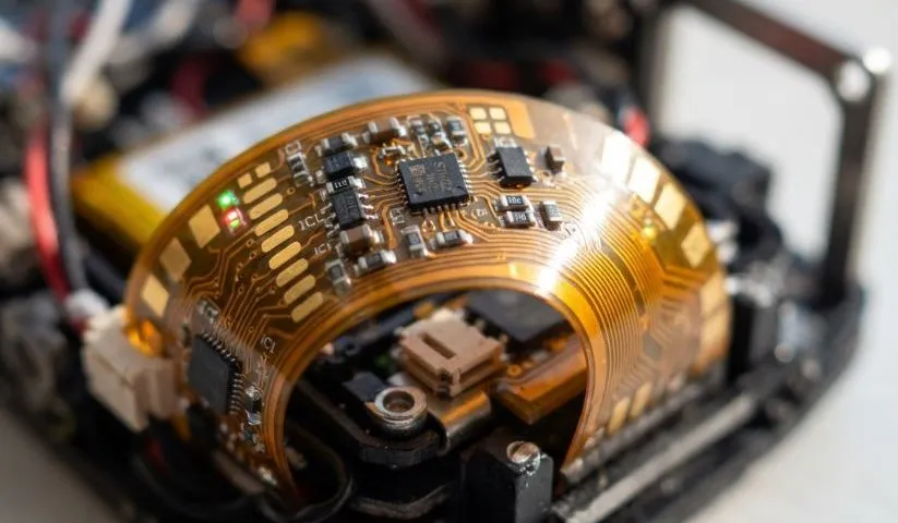
For those of you who may not be familiar with the term flexible printed circuit boards you have visited the right place!  They are simply printed circuit boards (the electrical brain of computers) that have the ability to bend or flex making them wearable.  Once you understand this the name makes perfect sense and is self-explanatory.  Generally, they are uses in type of electronic device that needs to be flexible during its use.  They are separated into three separate classes each with specified uses that make them unique.

Class I (One)

Class I flexible circuits are a part of every type of device that you can conjure up.  They do not need a whole of attention while wearing them because they are not exposed to rough environmental factors that usually results in the malfunction of the device.  Some examples of flexible PCB devices would be halter monitors (measures your heart rate), calorie counters, and devices that measure the number of steps you take during the time you are wearing the device.  The standard that must be met for this class is based on reliability and quality.

Class II (Two)

Class II flexible printed circuit boards are utilized for industrial and commercial industries.  They also are not usually exposed to tough environmental factors because of this their standards are based on quality and efficient solder joints making connections within the circuitry.  An example of where you will find a flexible PCB would be in a home automation system.  Most home systems allow you to communication with certain appliance through the internet.

Class III (Three)

Class III flexible printed circuit boards are used for military, aerospace, and medical electronics.  Since these boards are used for such important tasks their standard requirements must meet an extremely demanding testing process before they are deemed ready to function.  The assembly process is also more involved when creating them;

  • Knowing when and how to connect the vias in the bend areas
  • Avoid connecting vias when possible
  • Assuring stiffeners stay in the right places
  • Bending and twisting at different ratios, angles and levels
  • Different electrical components that are associated with it
  • Different thermal traits
  • Application of the J Standard to all military devices
  • Environmental testing
  • Thermal Shock cycling
  • Temperature cycling

Flexible PCB’s are the very heart of computerized machinery, without them we would not be able to enjoy our cell phones, games, computers, the list can go on and on!  We have come to depend on our devices, understanding the types of circuit boards your electronic gadgets have will help you appreciate those wonderful fabricators or manufacturers who share their expertise with the world so we can benefit from everything technology has to offer.  Whether you are using class one, two, or three, or any combination of the three you have experienced what todays flexible printed circuit boards have to offer us.  We excitedly continue to look forward to see what today’s technology will bring us next.

Causes PCB Failure

What Causes PCB Failure

What Causes PCB Failure

PCB failure occurs whenever there is a disturbance that affects your printed circuit board; it can be caused by many different variants. The usual suspects are moisture, heat, and dirt.  It may not always be easy to avoid, however keeping your board as clean as possible will go a very long way in keeping it up and running.  Factors such as prototype layout issues, assembly errors, and invalidated circuits can cause discrete or power component failure, and trace damage that will cause your printed circuit board to fail.

Prototype issues or first run issues can sometimes play a role in the malfunction of your PCB.  For example, if they are missing traces or vias your PCB will not be able to function properly.  The following have also been known to cause disruptions in PCBs, traces are too small, noise, incorrect pad sizes or footprints, mechanical fit and placement of mounting features all play a role in the malfunctioning PCB.

Assembly errors are also among the evils that cause failures.  Such as the wrong PCB manufacturer, change of materials and layers, will affect the PCB and place an entire project at risk.  Additional causes may also be placing the component in backwards, components installed in the wrong place, bent leads, cold solder joints, no solder, solder mask problems, defective, out of tolerance, mismarked components, and a marginal circuit design.  These can all lead to PCB failure right out of the gate as well as a lot of aggravation and frustration. Another issue can be circuits that were not validated such as sixteen volts in a twenty-four-volt power supply.

Discrete component failure can occur through the natural aging process, overheating, and electrical surges, risers in ESR values, and corrosion and drying.

Power component failure can occur through aging, electrical surges, and overheating.

Trace damage failure can occur through electrical surges, lightening, inappropriate assembly, and metallic dust.

You will not always be able to see these problems just by looking at your board, it may sometimes be necessary to check it with a meter to see what the problem is.

A burnt component is another common issue that will cause your PCB to fail.  This occurs when the device has overheated.  Any change in temperature can cause a malfunction; make sure you have enough space around your device to allow air to flow in and out freely.

Age also plays a role in the function of your PCB.  As with everything the natural process of aging affects the performance of your device.  Changing out the old parts is a generally easy task to perform as long as you really know what you are doing.

There a many factor’s that can play a part in your printed circuit boards failure. They can be simplified into two categories, environmental and manufacturing.  Making sure you chose a reputable PCB manufacturer will help ensure that you receive the PCB you require.  Contact Rush PCB engineers today to find out how they can help you.

Reliable PCB Assembly Services

Assembling Wearable Electronics

Assembling Wearable Electronics

Rush PCB Uk engineers know the importance of keeping up with all of the latest technological advances of the times.  With the constant introduction of new technology staying current in the contemporary market is a necessity for our customer’s satisfaction and our continual growth.  For example, the demand for wearable electronics is at an all-time high, with such popularity it is necessary to be constantly on the look-out for new and better ways of improving functionality as well as the assembly process.  Whether we are assembling smart watches, tracking devices or medical alert devices, Rush PCB experts understand their complexity and the precision necessary to successfully assemble the device to function correctly.  As a matter of fact, the assembly of wearable electronic devices does not differ greatly from the assembly of other types of printed circuit boards with the exemption of the size.

Aside from their difference in size, wearable PCBs can also come in various shapes and sizes, which can make the assembly process a bit more challenging.  Their smaller size requires much more attention to detail and exact precision.  Our engineers love challenges, we are ready to begin any wearable electronic assembly and guarantee that you will be satisfied regardless of the shape and size of your PCB.  By using a heat-curing adhesive to join the flex circuits to a rigid board our engineers ensure that the difference in the coefficients of thermal expansion are balanced so the sensors will operate as expected.  The final product will provide a flat even that provides enough surface tension to control solder paste spilling while including techniques like overprinting and under-printing.

Understanding the importance and sensitivity of sensors PCB engineers design soldering pads which enable the sensors to come in contact with skin so they can collect the information they were designed for.  This is just one consideration in our process.  Other factors included in assembly are the direction of the bend of the circuitry, degree of bend, number of fold cycles, application type of the device.  When assembling wearable electronics, our experts provide quality devices guaranteeing that they will bend and twist so the wearer of the device will be able to perform their normal activities without damaging it.  From stencil printing to the thermal profile or reflow, Rush PCB UK  provides quality devices that you can count on.

During the stencil printing phase our engineers guarantee that the distribution of solder paste is perfect ensuring that the appropriate electrical connection is achieved.  When we move on to the pick and place phase, we precisely position the components, the surface of the flex-circuit, surface mount pads through the use of specifically designed fixtures and special tooling.  Shields and cages are delicately placed during the pick and place phase.  For the thermal profile or reflow phase, the most challenging one of all, our engineers lower the temperature of the conduction oven, using special profiling care for lead-free wearable electronics.  Contact us today to find out how we can help you.

pcb_layers

Multilayer Printed Circuit Boards – Multilayer PCB With Latest Technology

Advantages and Challenges of Multilayer PCBs in Modern Electronics

Traditional single-sided Printed Circuit Boards (PCBs) cannot meet the needs of increasing assembly density requirements as they have reached a functional limit of available space. Double-sided printed PCBs are also subject to the same physical constraints.

Multilayer PCBs have been developed to address these space issues. Multilayer PCBs are used in a range of professional electronic products ranging from everyday computers to complex military equipment. Multilayer PCBs are especially useful in circuits designed for high-speed use. They provide benefits in reducing the risk of overloading based on weight or volume and provide additional space for conductor patterns and power.

Multilayer PCBs are now widely used in a broad range of electronic devices. They have become a crucial part of electrical components as they offer many advantages. Some of these include flexibility, reliability, small size, high assembly density, and the use of shielding layers for electronic and magnetic circuits. They provide a useful tool for high-speed transmission requirements. Once they have been produced and tested, they are relatively simple to handle and install.

In terms of configuration, multilayer PCBs are made up of two (or more) ‘traditional’ PCBs that are stacked together. They are connected with pre-defined mutual connections. A single multilayer PCB will have at least three conductive layers. These are the two ‘outside’ layers, and at least one layer has been synthesized in the insulation board.

The development of multilayer PCBS generates problems that aren’t relevant to single- or double-sided PCBs. These included stray capacitance, crosstalk, and noise. The design of multilayer PCBs must take these factors into account. Development processes include avoiding parallel routing and minimizing the signal line length. When multilayer PCBs are designed with an understanding of the risks of noise, capacitance, and crosstalk, and manufactured using state-of-the-art equipment, close-tolerance PCBs can be manufactured with a range of layers to meet various specifications. Some boards can be built with up to 16 layers, while if required, the process can be used to design and manufacture boards with up to 28 layers, with a maximum thickness of 3.2mm. As the technology used to design and manufacture multilayer PCBs continues to improve, they will become commonplace in many use fields.

The specifications for producing multilayer PCBs are no different from those of single layers. They can be produced on all recognized PCB industry surfaces and can use high-frequency base materials for applications up to 80 GHz.

Cost is a factor that needs to be considered when designing multilayer PCBs. The manufacturing process is more complex and the production runs are shorter. There is also a longer production cycle and more issues associated with testing. Traditional testing methods using single-layer PCBs are significantly more challenging when testing multilayer PCBs. As a result, the cost of multilayer PCBs will be proportionally higher than the cost of traditional PCBs.

All-In-One Contract Electronic Assembly

All-In-One Contract Electronic Assembly: Reducing Your Expenses

Advantages of Using an All-In-One Provider for Electronics Assembly

Historically, companies used outsourced production materials from various suppliers. The need to ensure all components of the final product are brought together promptly, with consistent quality means that there is increasingly an advantage to consider using an all-in-one supplier.

Electronic systems are increasingly impacting on our daily lives. Many things that we use regularly have increasing requirements for PCBs. For example, motor vehicles historically had minimal requirements for microprocessors. However, 15-30% of the cost of modern motor vehicles is in microprocessors. There is an increasing demand for PCBs, and they need to be high-quality reliable, and cost-effective. There are several reasons for considering using a single source for electronic assembly.

Equipment Expenses

Smaller electronics companies can be challenged by a lack of funding or a lack of resources. Machinery and equipment are constantly being upgraded. Larger companies can budget for regular updates of their equipment, while companies that don’t offer a comprehensive service may struggle to afford the newer equipment. As a result, they may be less capable of providing the highest quality and most cost-effective products.  In contrast, larger manufacturers will be able to amortize the cost of upgraded equipment over a shorter time frame and can upgrade more frequently.

Larger Scale Production Runs

Contract manufacturers with more up-to-date equipment are more likely to have the scale and capacity for delivery of larger production runs and will be able to meet your requirements for timely delivery.

Integrated Quality Control

Quality control is an essential aspect of PCB manufacture. An all-in-one provider will work with you through the design, testing, and printing processes to ensure that your printed PCBs meet the market requirements and that the device that the PCBs used in functions in line with your plans.

Options for Sourcing Components

An all-in-one provider will have a wide range of components that ensure the parts you require are readily available. While many companies can provide components that are of a similar standard. The cost per unit may be insignificant, but the overall cost of production may provide significant financial benefits.

Integration of Prototyping

Many manufacturers do not provide prototyping. The need to use a third party for prototypes will add time and potential risk to your project. Using an all-in-one provider will allow for more effective iterative design from the prototype, allowing more control over the design process.

Special Requirements

In the past decade, there have been significant changes in board design. You may require a board with SMT. Maybe your board needs to be a Flex or Rigid Flex design. It could be that you need special requirements based on the environment that your board will be used in. Dusty, hot, damp, or cool environments may all affect performance. An all-in-one provider will understand these issues, and plan your production to meet your special requirements.

When you weigh up all the factors, you will see that it makes sense to use an electronics assembly provider who can provide an all-in-one service.

Essential Parts of a Printed Circuit Board

Essential Parts of a Printed Circuit Board

Understanding PCB Components: Traces, Layers, and Functionality

To have a thorough understanding of Printed Circuit Boards (PCBs), it is important to know the various parts that are used to make the boards.

The most obvious starting point is the board itself. It is plastic, reinforced with glass. The next most obvious parts are the lines and pads that connect together. These are made of copper, and are known as ‘traces’. They conduct electricity, allowing electrical charges to be carried through the board. They are similar to wires, but are much finer, and are used to carry the electricity to the end-point (one of the various types of components within the board).

Simple PCBs are single-sided, with one copper layer. These are structured with one side having all the components, while the other side had the traces. Holes are placed through the board for the circuit to be carried from the trace to the component. For many years, all boards were made in a single-sided design. By definition, double-sided PCBs have traces on both sides of the board.

To allow the boards to be more complex and control additional functions, multi-layer boards are used. Additional layers of board have their own set of traces and components. In developing multi-layer boards, a range of issues needed to be addressed. Firstly, it is essential that the copper connections do not cross each other, as this would compromise the path of the electrical circuit. Other factors that need to be considered are resonance and noise and capacitance.

The layer set in place above the copper is called the soldermask. This is a form of insulation, ensuring that the copper traces aren’t affected by any metal that may come into contact with it. It is traditionally colored green. It is designed to have gaps that expose the copper in specific places, providing points where components can be soldered to the board. The silkscreen is a layer that is printed onto the soldermask. It is a layer where text can be printed (letters and numbers) that provide instructions for the user.

A range of components can be incorporated into a PCB. Without components, the PCB is simply a conductor of electricity, with no function. Components can be grouped into two broad categories – passive (components that do not require direction) and active (components that only function when they receive current from one direction). Common components include:

  • Batteries: these provide the circuit with voltage.
  • Capacitators: The store electricity for later use. They are available as polarized or non-polarized.
  • Diodes: allows current to pass in one direction only, blocking the other.
  • Inductor: These coils store charge in a magnetic field.
  • Light emitting diodes (LEDs). These light up when current flows is applied. They only allow current to flow in one direction.
  • Resistors: These control the electric current as it passes through. The level of resistance provided varies based on the needs of the engineer. They are made in different color codes to show the level of resistance.
  • Switches: These can be open or closed, allowingor blocking current.
  • Transistors: These are a form of switch that performs changes function based on the voltage passing through.
  • Vias: small holes in the board that allow a signal to be passed from one side to the other
High Frequency Board Design

High Frequency Board Design – What You Need to Know

Designing High-Frequency PCBs: Mitigating Electromagnetic Interference (EMI)

A factor that engineers need to consider when designing PCBs is Electromagnetic Interference (EMI). This occurs when there is a disturbance generated by an external source which affects the electrical circuits. This interference may be through electromagnetic induction, electrostatic coupling, or conduction.

When high frequencies are involved, the level of EMI occurring within a PCB trace and in components increases. It is important to remember that every device, trace and via can act as a source of EMI. Boards are considered to be high frequency when the signal is greater than 3 MHz, and is rapidly changing.

It is important when designing any PCB to follow basic rules of component placement, but even more so when considering high frequency boards. The order should be:

  1. Connectors;
  2. Power circuits;
  3. Sensitive and precision circuits;
  4. Critical circuit components;
  5. Everything else.

A DRC will only be able to identify errors that it is programmed to monitor. Many of the issues associated with high frequency boards will pass through a DRC check, as they are not functionally ‘errors’. Things to watch in DRC checking include package-to-package spacing, shorted or unconnected nets, and air-gap violations. When considering the PCB layout, there are many factors to pay close attention to:

Trace:

It is also important to consider trace widths when planning high frequency boards. Trace widths of 10 to 20 mils are used for traces carrying 10 to 20 mA; while trace widths of 5 to 8 mils should be used for traces carrying less than 10mA.

Routing:

The routing also needs to be carefully considered, as does the need for high-impedance nodes.

Placement:

It is important to consider the placement of sensitive nodes and circuits. They will need to be shielded from sources of noise. A solder mask should be in place between pins and vias. It is also essential that the silkscreen is clear and concise.

Layers:

It is recommended that the first inner layer below the component sides is used as ground. Other layers should then be assigned power planes. Stack-ups need to be planned in a way that balances the board around the midpoint of the Z axis.

Transmission Lines:

There are two common structures – microstrip and stripline circuits. Both have different properties, and the preferred layout should be tested to ensure it meets your specific needs. Microstrip designs may be subject to crosstalk. To minimize crosstalk on adjacent traces, the traces should be separated by at least twice the trace width.

If the circuit is differential, the traces for both signals need to have the same length to ensure that propagation delay times are equal, ensuring that the electromagnetic fields effectively cancel each other out.

As with all PCB design, it is best to have the design reviewed on an ongoing basis through the design stages, with adjustments made iteratively to ensure the EMI impacts are minimized in the high frequency board.

pcb supplier

PCB Suppliers Working With Industry

The Role of PCBs in Today’s Electronic Environment

In today’s electronic environment, PCBs are everywhere. Daily, we work with items that include circuit boards in almost every electronic device. Think of the following situations where many people are likely to encounter PCBs on a regular (and probably daily) basis:

  • Motor vehicles;
  • Cell phones;
  • Tablets and computers;
  • Household appliances;
  • Office equipment;
  • GPS navigation systems;
  • Home exercise equipment;
  • automatic

PCBs are everywhere in the corporate world and industry as well, in situations such as automatic lighting and heating systems, medical equipment, hearing aids, home health monitors, home handyman tools such as snow blowers, manufacturing plants, trains, and planes… the list doesn’t stop! The US market for PCBs and component manufacture was estimated to be $44 Billion in 2014.

Bearing this in mind, the world of technology is changing more rapidly than most people ever imagined. As a result, technology is moving in new directions that had not been contemplated just a few years ago. There are implications for people, for industry, and for the providers of technology components.

If you take your mind back a few years, technically adept owners of home computers could open the lid and repair, upgrade, or possibly even build systems. More recently, manufacturers have put protocols in place that mean such actions risk of canceling factory warranties. Because of this, businesses that operate as small to medium electronic manufacturing and repair services have the opportunity to expand in two areas – licensed electronics and licensed computer repairs.

Tier I electronic manufacturers provide services to original equipment manufacturers. Tier II manufacturers provide services to Tier I organizations. Companies in both tiers are now looking for supply chain partners. A key area of the supply chain is having reliable circuit board suppliers. Suppliers of PCBs are being asked to develop processes that provide instant access and rapid shipping to customers anywhere around the country, and beyond.

Ideally, circuit board suppliers will have a team who are knowledgeable and informed. Companies with good staff can help their customers make informed decisions about PCB design requirements. They can also guide the policy and practice of PCB supply. They should be able to provide standard hard-board designs and flexible PCBs. Companies operating in this space will also need to be able to provide a range of service options for customers, including delivery of some or all parts of the design process. They should be able to provide quotes quickly and with sufficient detail for their clients to be able to easily understand the available choices.

The success of these companies can be directly linked to the identification of suppliers of the best products and components. With a poor supply of products, there is always a risk of a failure of a PCB. Such failures can be associated with two common causes: issues that weren’t identified in the design stage of the PCB production; or performance issues that are related to environmental stresses in the operating location of the PCB such as cold, humidity, heat, or dust.

The real goal of PCB suppliers is to ensure that customer can create their products without concern for the logistics and processes of ensuring the availability and quality of the PCBs. Tier I and II manufacturers may now have the capability of checking the quality integrity of all suppliers, especially if they operate offshore. However, a supply chain distributor can provide such checks. Larger suppliers can create a delivery and inventory system that helps ensure that end customers avoid the headaches of international shipment logistics. Through the use of a distributor of this nature, good PCB suppliers can ensure customers have a focus on what they do well – delivery of service in their sector of the technology market.