PCB Manufacture 2

Why RushPCB UK Is a Reliable PCB Manufacturing Company

Why RushPCB UK Is a Reliable PCB Manufacturing Company

Consumer demands and industry challenges are increasing tremendously towards lightweight products, miniaturisation, greater product design freedom, lower costs, more environmental friendly applications, and higher reliability. In all these aspects, flexible circuits from a trusted PCB manufacturer UK, RushPCB, are proving their worth.

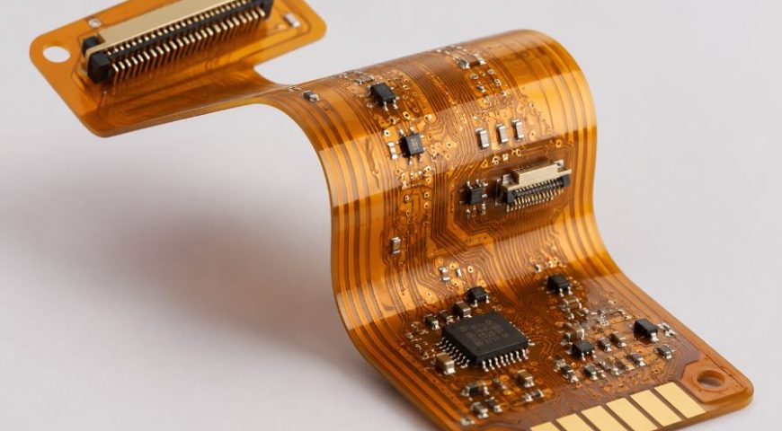
Flexible Circuits from RushPCB UK

The flexible circuit technology offers a huge range of benefits and capabilities. Offered by the best PCB manufacturer UK, flexible circuits effectively eliminate wiring errors commonly associated with manual wiring harnesses, which simplifies assembly. As these circuits can flex, form, and bend to follow the contours of cabinets, they often eliminate several connectors, reducing component numbers, assembly effort, and time. All this goes to increase the product reliability.

RushPCB, a reliable PCB manufacturer UK, makes high-quality flex circuits that encourage 3-D packaging through their property of dynamic flexing. The circuits offer unmatched high speed and high frequency performance as they allow excellent control over transmission impedance, while offering lower impedance as compared to that offered by conventional wiring.

RushPCB offers flex circuits with dielectric substrates that are good conductors of heat. This improves heat dissipation, while flat conductors provide thinner circuits, leading to a huge improvement in airflow capabilities. Additionally, the compliant substrate minimises thermal mismatches.

The lightweight nature of flex circuits helps in reducing the weight of the product, which in turn, the OEMs can use for increasing their products’ packaging density, aesthetics, appearance, or for offering designs that are more integrated.

Advantages of Flexible Circuits from RushPCB UK

There are several benefits of using flexible circuits from the most trusted PCB manufacturer UK. RushPCB offers the thinnest dielectric substrates, as thin as 0.002 inches, and these reduce the package size and weight extensively—sometimes by as much as 75%—the weight reduction being especially attractive to the aerospace industry.

By using flexible circuits, OEMs can bring down their assembly costs. They achieve this in two ways—first, by reducing the number of assembly operations required, and second, by their ability to test the circuit before committing it to the final assembly. This comes from the highly reliable design of flexible circuits from the best PCB manufacturer UK, RushPCB, as their design offers an excellent means of reducing the number of levels of interaction required by the product.

Hand-built wire harnesses do ease the assembly process, but often introduce wiring errors that take up troubleshooting and repair time. Flexible circuits eliminate wiring errors entirely, as it is not possible to route them to points other than those already designated.

pcb

SMT and Flexible Circuits Assembly

RushPCB, the best PCB manufacturer UK, offers flexible substrates, and uses the most advanced surface mount technology (SMT) components and reliable conductive lead-free solder pastes for mounting them. Flexible circuits from RushPCB come with highly compliant substrate material that effectively counteracts the effects of thermal stress, as SMT components are highly sensitive to thermal mismatch between the component material, mounting, and the substrate.

High Density Interconnect PCBs from RushPCB

For customers requiring even higher wiring density per unit area, highly trusted PCB manufacturer UK, RushPCB, offers the High Density Interconnect (HDI) PCB technology. HDI technology offers finer lines and spaces, smaller vias, capture pads, and higher connection pad densities than conventional PCB technology can. OEMs use HDI PCBs to reduce the weight and size of their products, while enhancing their electrical performance.

RushPCB makes HDI PCBs using microvia and buried via technology, along with sequentially placed lamination, insulation material, and conductor wiring layers for very high density of routing. Coming from the best PCB manufacturer UK, RushPCB, HDI PCBs are the best alternatives to expensive high layer-count standard laminates or sequentially laminated boards.

Signal Integrity in HDI PCBs

For high-speed boards, maintaining signal integrity is highly desirable. For this, the PCB has to possess excellent AC characteristics, such as high-frequency transmission capabilities, impedance control, and low radiation. Furthermore, stripline and microstrip transmission line characteristics necessitate a multi-layered design.

To maintain signal integrity, the insulating material in the PCB must have a low dielectric factor along with a low attenuation ratio. Unprecedented high-density is demanded by mounting and assembly methods for Direct Chip Attachment, Chip Scale Packaging, and Ball Grid Array packages. RushPCB achieves these using the microvias and buried via technology, which uses holes with diameters down to 150µm and even lower. Rather than use regular drill bits, RushPCB prefers to use highly accurate lasers for drilling such small-diameter holes.

Advantages of Using HDI PCBs

The HDI technology from RushPCB offers substantial advantages over regular PCBs—making products smaller and allowing high-speed and high-frequency operations possible. HDI offers compact boards that give better electrical performance and lowers the power consumption. Shorter connections mean better signal integrity and other performance improvements due to minimal stubs, closer ground planes, lower EMI/RFI, and distributed capacitances.

rush pcb

RushPCB is Internationally Certified

OEMs, when selecting a consultancy for circuit board manufacturing, look for those with certification to international standards. Trusted PCB manufacturer UK, RushPCB, conforms to IPC-A-600, and the standard defines the acceptability of circuit boards for quality of workmanship and sets the comprehensive criteria for their acceptance.

That means RushPCB as PCB manufacturer UK produces quality products and identifies sources of non-conformance, if any, in their manufacturing processes. RushPCB conforms to the IPC-A-600 training and certification, and therefore, the manufacturing services reduces the risk of mounting expensive components on PCBs that are defective. This not only reduces scrap, but also facilitates better communication with OEMs.

As a trusted PCB manufacturer UK, RushPCB employs experienced engineers, purchasing professionals, and quality inspectors to define PCB requirements properly, specify requirements for purchasing, and to detect non-conformances. If you are looking for a reliable PCB manufacturing company, as a trusted PCB manufacturer UK, RushPCB will fulfil all your requirements.


rushpcb uk 2

PCB

Secrets of High Speed Printed Circuit Boards

Design for Assembly in Fast PCB Prototyping

In our fast-paced world, OEMs need to churn out new electronic devices very quickly to remain in the forefront of the market. For this, they require rapid PCB prototype services, which allow them to test their new designs thoroughly. Once they are ready to enter the market, OEMs need to tie up with a fast PCB production partner to fulfill the marketing demands. If the design requires high-speed printed circuit boards, the design house cannot afford the time to make trial and error, but must optimize the design on the first try. This ensures a smooth quickturn PCB production process. Therefore, the designer must start designing the board with assembly in mind.

Design for Assembly

Whatever be the type of PCB involved—rigid, flex, rigid flex, high density interconnect (HDI), or conventional—the bare boards will require assembly with additional components, before they are useful. Usually, the assembled PCB fits within a product or application, and overlooking this aspect of the assembly during design may ultimately lead to significant complications.

High Speed operation of PCBs requires the designer achieve the following:

  • Minimizing noise generation from the on-board power network
  • Minimizing cross-talk between traces
  • Reducing simultaneous switching noise
  • Proper impedance matching
  • Proper signal line termination
  • Reducing the effects of ground bounce

Board Material and Transmission Line Design

The dielectric construction material of the PCB is a major contributor to the amount of noise and cross talk the fast switching signals generate. A high frequency signal traveling along a long trace on the PCB could be affected seriously if the loss tangent of the dielectric material is high, resulting in high absorption and attenuation at high frequencies.

The modeling and effect of transmission lines also affects the signal performance and its noise separation. In general, any circuit trace on the PCB will have its characteristic impedance. This depends on the trace width, thickness, the dielectric constant of the PCB and the separation between the trace and its reference plane. Designers can route circuit traces on a PCB in two ways—in a microstrip transmission line layout or a stripline transmission line layout.

In a microstrip layout, the designer routes the circuit traces on an outside layer with a reference plane below it. The characteristic impedance of a circuit trace in a microstrip layout is inversely proportional to the trace width, and is directly proportional to the separation from the reference plane.

In a stripline layout, the designer routes the circuit traces on an inside layer of a multi-layer PCB, with two reference planes on either side. Here again, the characteristic impedance is inversely proportional to the width of the trace, and directly proportional to the separation from the reference planes. However, the rate of change with trace separation from the reference planes is much slower in a stripline layout as compared to that with s microstrip layout.

Designers for rapid PCB prototype services must be able to predict the characteristic impedance of their design if they are to get their design right the first time. Understanding the nuances of transmission lines helps with fast PCB production.

pcb-01

Minimizing Cross-Talk between Traces

While designing a high speed PCB, designers must take steps to reduce cross talk between neighboring signal lines, even when following either the microstrip or the stripline layout. Designers follow certain thumb rules to minimize the cross talk:

  • Utilize as much space between signal lines as the routing restrictions allow
  • Place the transmission line as close as possible to the ground reference plane
  • Use differential routing techniques for critical nets—match the length to the gyrations of each trace
  • Route single-ended signals on different layers to be orthogonal to each other

Routing two or more single-ended traces in parallel with not enough spacing will increase the cross talk between them. Therefore, designers prefer to minimize the parallel run, often routing them with short parallel sections, minimizing long, coupled sections between various nets.

Maintaining Signal Integrity

For high-speed boards, it is very important that the signal maintains its integrity, that is, it is able to keep its amplitude, and shape as it travels from its source to its destination. Signals may be single-ended, such as clocks, or may be differential, which are very important for high-speed design. For traces carrying single-ended signals, designers follow design rules such as:

  • Keeping traces straight as far as possible, and using arc shaped bends rather than right-angled bends where necessary
  • Not using multiple signal layers
  • Not using vias in the traces—they cause reflections and impedance change
  • Using the microstrip or the stripline transmission line layout
  • Minimizing reflection by terminating the signal properly

Designers follow additional rules for differential signals:

  • Minimize crosstalk between two differential pairs with properly spacing them
  • Maintain proper spacing to minimize reflection noise
  • Maintaining constant spacing for the entire length of the traces
  • Maintaining the same length of the traces as this minimizes phase and skew differences
  • Not using vias in the traces—they cause reflections and impedance change

Effective Filtering and Grounding

Conducted noise from the power supply can hinder the functioning of a high speed Printed Circuit Board. Since a power supply may deliver noise of high as well as low frequencies, designers minimize this problem by effectively filtering the noise at the points where the power lines enter the PCB,

An electrolytic capacitor across the power lines can filter the ripple and low frequency noise, while a non-resonant surface ferrite bead will block most of the high frequencies. Since the ferrite bead will be in series with the supply lines, its rating needs to be adequate to handle the current entering the PCB. Designers also keep provision for a decoupling capacitor very close to each IC on the board, to smoothen out very short duration current surges.

Effective power distribution throughout the PCB is extremely important for printed circuit boards operating at high speeds. For doing this, designers often use power planes or a power bus network. Power planes on a multi-layer PCB comprise two or more copper layers carrying power to the devices—typically, the VCC and GND lines. By making the power planes as large as the entire board, the designers ensure the DC resistance is as low as possible.

This offers multiple advantages to high speed boards—high current source and sink capability, shielding, and noise protection to the signals. For two-layer PCBs, designers often use the power bus network, which has two or more wide copper traces for carrying power to the devices. Although the DC resistance of the power bus is high compared to power planes, they are less expensive.

rushpcb uk-01

As high-speed digital devices operate simultaneously, their fast switching times may cause a board-level phenomenon known as ground bounce. This is a very difficult condition to predict, as several factors may influence to the occurrence, such as number of switching outputs, socket inductance, and load capacitance. Designers follow a number of broad guidelines to reduce the effects of ground bounce:

  • Placing vias adjacent to a capacitor pad, and connecting them with wide, short traces
  • Using wide, short traces to connect power pins to power planes or decoupling capacitors
  • Using individual links to connect each ground pin to the ground plane, no daisy-chaining
  • Adding decoupling capacitors for each IC and each power pin
  • Placing decoupling capacitors very close to the IC
  • Properly terminating the outputs to prevent reflections
  • Buffering loads to limit the load capacitance
  • Eliminating sockets as far as possible
  • Distributing switching outputs evenly throughout the board
  • Placing ground plane next to switching pins
  • Using pull down resistors rather than using pull up resistors
  • Using multi-layer PCBs with separate VCC and GND planes
  • Placing power and ground planes next to each other to reduce the total inductance
  • Minimizing the lead capacitance by using surface mount devices
  • Using capacitors with low effective series resistance

rush pcb

Conclusion

Rush PCB UK recommends designers follow the above design guidelines for delivering rapid PCB prototype services to satisfy customers. However, please note that all other general guidelines for PCB design are also important and designers should follow them meticulously for fast PCB production.

Flex pcb 2

How Stable are the Dimensions of Flexible Circuits

Compensating for Dimensional Changes in Flexible Circuit Fabrication

The difference between a rigid printed circuit board and a flexible circuit lies in the dielectric material sets manufacturers to use for fabricating them. Most rigid printed circuits are made from glass epoxy, whereas the material of choice for a majority of flexible circuits is Polyimide. The development of several versions of polyimide enables tailoring the material to meet specialty requirements such as in solar arrays, space applications, and other unusual environments.

Although it is possible to form glass epoxy in very thin constructions and even bend it for simple applications, polymer films are most suitable for continuous twisting, flexing, and multi-planar folding. Films of polyimide withstand numerous bending cycles without suffering any degradation of their mechanical and electrical properties. Therefore, polyimide films perform reliably in applications where bend cycles of over a million are common. The inherent flexibility of polyimide films offers the electronic packager a wealth of design options. However, a disadvantage of polyimide films is their material dimensional stability is inferior to that of glass epoxy materials.

Dimensional Stability

According to manufacturers, the dimensional stability of polyimide films depends on the residual stresses the manufacturing processes place in the film and its normal coefficient of thermal expansion.

However, the measure of stability represents only the effect of the film alone. The nature of stability grows more complex as the fabricator exposes the film to elevated temperatures and pressures for attaching the copper layers through processing to create an adhesive-less laminate, or through an adhesive lamination cycle. However, the process of creating a laminate and subsequently fabricating a circuit involves two different processing effects, and during each of these fabricating processes, the flexible substrate undergoes dimensional changes.

It is not easy to predict these changes. Raw material variation from batch to batch may cause dimensional changes to vary slightly. Changes also depend on the method of construction and processing conditions, as thin materials are likely to be less stable. Other contributing factors can be the percentage of copper etched, density of copper electroplating, ambient humidity, and material thickness.

Small dimensional changes in the circuitry panel are inevitable as it undergoes processing and exposure to a variety of etching, electroplating, pressures, temperatures, and chemistries. For instance, each shrink is the stress etching copper releases, but fabricators mistakenly use it as a catchphrase for representing all the dimensional changes that a flexible circuit undergoes during processing.

Fabricators consider compensating for the above changes when setting up the part number for a new flexible circuit. However, accurate prediction of these feature movements requires empirical data from the parts they produce.

rushpcb uk 2

Effects of Material Instability

Lack of stability in the film material is manifest in violation of the minimal annular ring requirement, and in extreme cases, causes a full breakout of the hole-to-pad alignment. Another possibility is in the misalignment of the overlay. For a predictable material change, the operator can adjust either the conductor layout or the drill pattern to re-center the plated-through hole in the pad.

Dealing with Dimensional Changes

Fabricators deal with dimensional changes by limiting the panel size, and this works very well for cases where the tolerances are extremely tight. In small panel sizes, the effects of dimensional instability issues on registration and alignment are lower, and the handling damages are at a minimum. However, smaller panel sizes may be less efficient for processing as those for larger panels, since in a circuit factory several costs are based on panel size.

Compensating for Dimensional Changes

It is possible to achieve cost-effective production with suitable panel sizes while compensating for dimensional changes. Fabricators can adopt the following methods to adjust for dimensional changes occurring during circuit fabrication:

Applying Scaling Factors

Where the dimensional changes of the material are predictable, fabricators can apply scaling factors to tooling or secondary layers. The in-process measurements for a given lot can allow fabricators to use scaling factors based on dynamic calculations. For instance, the measured scaling factor of a panel may form the basis of the creation of its solder paste stencil. Another instance may be of a final drilling program compensated dimensionally for a multilayer circuit.

Applying Software Compensations

Alignment systems using software-controlled operations can use optical fiducials to detect dimensional shifts and compensate for them. Such fabrication machines measure these targets present on the outside corners of the panel and perform a dimensional analysis. Proper alignment is then a process of applying the necessary X, Y, and theta corrections.

rushpcb uk-01

Processing Sub-Panels

Fabricators often divide the panel into smaller arrays for handling dimensional changes. They do this usually after creating the circuit image. As the processing is on subsets of the panel, fabricators effectively gain some of the advantages of small panel alignment, but without compromising the cost advantages of processing a large panel.

Fabricators typically use optical targets on smaller subset panels to compensate for stencil registration commonly. They also use hard tool dies to cut smaller pieces at a time from a multi-piece panel.

Summary

Dimensional change is the primary difference between rigid and flexible circuitry, and this requires compensation. Even though the material change in flexible circuitry is typically less than one-tenth of one percent, it accumulates over a dimension of several units and can be significant. For a flexible circuit, this compensation for the expected change becomes a critical part related to penalization. This also serves to balance maximizing process efficiencies and maintaining dimensional tolerances and accuracy.

rush pcb

PCB Manufacture 2

How to Choose a Professional PCB Assembly Company

Transforming PCB Manufacturing: The Impact of Cloud Assembly Services

Hardware designers requiring PCB assembly in UK usually face tremendous obstacles to their need for prototyping and small batches. Large companies with huge inventory needs and long delivery horizons can wait for days or weeks for a proposal while accepting large minimum quantity requirements. For them, delays associated with overseas manufacturing are no big deal. However, these conditions are simply unacceptable for small industries, engineers, makers, and entrepreneurs.

A new approach to PCB assembly is gaining popularity. These PCB assembly services are also called kickstarter manufacturing or cloud manufacturing. For instance, RushPCB Inc., a PCB assembly company, now takes into the cloud activities such as quoting, sharing documents, ordering components, and other aspects of project management while working with PCB manufacturers. Customers can expect all interactions with the vendor streamlined and captured in real-time. Investors get the results they are looking for at reasonable prices. However, not all cloud PCB assembly companies are the same, and one has to look for the one that meets the specific requirements.

Best Practices of PCB Assembly Vendor

Selecting the professional PCB assembly company at the beginning determines the success of a project. Therefore, picking the right PCB assembly services provider becomes a highly important decision to be made. One must watch out for those offering very low prices, but subsequently are unable to provide the services, record of accomplishment, infrastructure, and technology to back up their promises. Rather, one must insist the PCB assembly services have the essential features, offer the services, and follow business practices such as:

rushpcb uk-01

Online Management and Reporting

The online administration portal of the PCB service provider is a window to the experiences as a customer. It should allow easy tracking and reporting on the progress of the project, make required changes, and upload design documents including the bill of materials. In short, it should allow the customer to check on the status of the product at any time, and from anywhere.

Instant Quotations

Waiting for days or weeks and trading a bunch of emails only to find out the cost of a PCB assembly, is not only a waste of time, it is expensive. A vendor offering instant, online quotations is always preferable. In general, although all vendors will start by sending a quotation for the project, therefore, selecting one who gets the process off painlessly is advisable. Moreover, selecting the vendor who gives an estimate in terms of quantity offtake helps in determining capital needs and product prices.

Prototyping Requirements

Most customers, before placing their order, want to be sure their PCB works exactly as intended. This may require making a few iterations to perfect the design. So far, prototyping was a big challenge under the old manufacturing model. However, PCB assembly in UK has progressed technologically, and there are PCB manufacturers willing to handle even a single quantity. Usually, vendors keep their prices in check by combining orders of low volumes into large production runs.

Minimum Order Requirements

Earlier, PCB assembly services were unable to accept production runs of small quantities. Older technology did not allow profitability in smaller numbers, which turned out to be a major challenge for everyone. However, use of modern technologies allows easy combination of small orders into larger ones, while switching from one task to another is no longer a major hurdle. Therefore, professional PCB assembly providers accept all types of order, regardless of quantity, and execute them at reasonable prices.

Seamless Manufacturing

With advancement in PCB assembly technologies, it is no longer necessary to track multiple vendors and suffer long lead times. A modern PCB assembly solution such as the Rush PCB Inc., offers a platform to upload design files, review and mange bill of materials, and resolve any assembly problems, online and from anywhere. Once the customer is happy with the design, the professional PCB assembly company takes over the sourcing, purchasing, and assembly of the components. Take care that the vendor offers access to updates on the platform and sends email notifications reporting the project progress. With this approach, expect the product to be available in days.

rushpcb uk 1

On-Shore Manufacturing

Printed Circuit Board assembly in UK can now offer prices competitive with offshore options, thanks to modern PCB assembly techniques. Therefore, enterprises selecting a PCB assembly partner based in the UK can expect to eliminate the delays, risks, costs, and complexity of dealing with a provider from overseas.

Looking Beyond PCB Assembly

The PCB happens to be only the first step of the many for most inventions and products. Professional cloud PCB manufacturers, such as the RushPCB Inc., offer even more. For instance, they will allow shipping in of components and materials for building complex products. They also have a warehouse attached to their manufacturing line, which allows a reduction in delays and shipping fees.

Most products will ultimately be shipped to end-users. Therefore, look for a professional PCB assembly partner who can keep products in their inventory and transfer them directly to end-users upon order. Some, including RushPCB Inc., even provide an API for directly integrating with the enterprise ERP or other e-commerce system.

PCB BOARD 15

How to Choose Military and Aerospace PCB Assembly Company

RUSHPCB UK: Premier Military and Aerospace PCB Assembly Services

RushPCB UK is one of the few printed board manufacturers and a military and aerospace-approved supplier providing MOD contacts-ready PCB assembly services. With our commitment to innovation and excellence, we comply with the highest quality standards to provide our customers with the most advanced circuit board technologies the industry can offer for military and aerospace assemblies. As a premier PCB manufacturing and assembly company, we offer our vastly experienced PCB capabilities and extensive materials selection, along with innovative equipment.

For any PCB assembly company to meet the rigorous demands of the military and aerospace industry, they should meet the following criteria:

  • Must have mil/aero certification and quality assurance systems
  • Must be capable of supplying highly specialized defense and aerospace PCBs
  • Must be able to transition seamlessly from fabrication to PCB assembly
  • Must provide an extensive selection of materials

Mil/Aero Certification & Quality Assurance Systems

At RushPCB UK, we have the necessary quality assurance systems in place, and our team has the requisite technical expertise to provide our defense and aerospace customers with high-performing and reliable PCBs and PCB assemblies for critical applications. We have ITAR-registered state-of-the-art facilities, and we are certified to meet all major Aero/Mil requirements.

Image 1-01

Highly Specialized Defense and Aerospace PCBs

Military and aerospace have rigorous PCB design criteria with requirements of high precision and performance. We use advanced PCB technologies to meet these rigorous demands. Our capabilities include 40-layer boards, sequential laminations, vias-in-pads, laser-drilled micro vias, copper up to 20 oz., oversized boards, small boards for antenna/microwave, cavity boards, and laser direct imaging.

Seamless Transition from Fabrication and PCB Assembly

We are the stellar one-stop solution for PCBs in the UK, providing small quantities, quick turn military and aerospace assemblies all under one roof. We do not charge for set-ups and stencils, and neither do we charge for any Non-Recurring Expenses.

Extensive Selection of Materials

For military and aerospace PCBs, material selection is an important aspect of design and manufacturing. This ensures superior reliability and performance in the most extreme environments and critical applications. We offer a huge selection of advanced materials for meeting the demands of the military and aerospace industry.

Best Space and Military Electronic Manufacturing Company

For electronics specifically, space is an unforgiving environment, as the conditions up there are vastly different from those on the surface of the earth. Electronic assemblies must function flawlessly not only after leaving the assembly line, but must also complete their life span without faltering—there is no concept of maintenance or servicing in space.

With electronic manufacturing companies developing and manufacturing complex electronic assemblies for missiles, satellites, and spacecraft, each electronic device must be customized for the specific requirements of the purchaser to ensure superior quality, affordability, and prompt deliveries.

rush pcb

When dealing with military and aerospace requirements, it is insufficient to produce decent quality products. Military and aerospace assemblies must be of only the finest quality capable of enduring the stringent conditions.

Therefore, NADCAP certified electronic manufacturing services with exclusive qualities are required to produce devices that can weather the challenges from space programs with the help of radiation toughened electronic assembly services. Manufacturers gain this certification to make sure the PCB assemblies they product conform to the military and aerospace specifications.

PCB Assembly Services Offered

Electronic manufacturing services with ISO-9000 and NASA certifications have in-house knowledge ensuring the following:

  • Fast PCB assembly services
  • Flying probe tests
  • Conformal coatings
  • 5σ – 6σ processing (less than 200 faults per million opportunities)
  • Experienced design and layout personnel
  • NASA trained soldering experts

Electronic PCB assembly and manufacturing services incorporate the above advanced manufacturing technologies in operation-critical services such as quality management systems to achieve competitive production within a short span of time. This is because high-reliability MOD and aerospace electronics demand the highest standards for quality, reliability, and conformance.

Rush PCB UK manufacture these assemblies with zero defects, and they function error-free for their entire lifetime, under the most severe environmental conditions including the most intense cold, high moisture content, and high temperatures.

Image 2-01

PCB BOARD COMP

Why PCB Manufacturing Companies Should Train Their PCB Technicians

Training the Technicians: A Necessity for Professional PCB Manufacturers

PCB manufacturing companies such as Rush PCB Inc. have come a long way from their earlier counterparts who conducted most of their operations manually. These professional PCB manufacturers now use sophisticated automatic machines for most of their operations. Therefore, there is no way a nonprofessional can simply walk in and start working in a modern facility manufacturing PCBs.

Components of printed circuit boards go through several complicated processes involving physical, chemical, and mechanical operations before the PCB can be certified as ready for dispatch to customers. As most professional PCB manufacturers are ISO 9001:2015 certified, regular training is part of their Quality Management System.

Professional PCB manufacturers offer all or part of a range of services that may include:

  • Design of multilayer PCB layout
  • Multilayer flex, rigid-flex, rigid, and HDI PCB manufacturing
  • Surface-mounted and through-hole assembly
  • Electromechanical and cable harness assembly
  • Final product assembly and automated testing services
  • Components purchasing services
  • Complete turnkey from design to finished product

Each of the above services requires trained personnel to execute their activities.

Design of Multilayer PCB Layout

Multilayer printed circuit board layout and design require powerful computer-aided design packages to take care of the intricacies of different layers of the design. Technicians working at this level require in-depth knowledge of design rules, routing traces, grounding planes, the difference between analog and digital grounding, and more. They must also be well-versed in working with the specific CAD software package the company uses. Additionally, they must understand the use and importance of different types of vias such as micro-vias, blind, and buried vias.

Multilayer Flex, Rigid Flex, Rigid, and HDI PCB Manufacturing

PCB manufacturing is a complicated activity involving a large number of operations. Technicians involved in these operations need sophisticated hands-on training in identifying materials, handling them, working with them on different sophisticated machines, and learning to identify faults.

For instance, only a trained technician can know the method of programming a baking chamber for the right temperature and duration or program a computer-driven drilling machine using data from the Gerber files sent over by the customer.

PCB manufacturing involves several chemical processes. Technicians need to be trained in operational safety and the proper use of these chemicals. They would also need to be trained in the proper use of personal protective equipment these activities require wearing.

pcb-01

Surface Mounted and Through Hole Assembly

Professional PCB manufacturing companies such as Rush PCB Inc. also offer assembly services, for which they employ highly trained technicians. These technicians are thoroughly trained in different fields of surface mounting activities such as in operating pick-and-place machines, reflow machines, and automated testing machines.

As they handle both passive and active components, the technicians need to be aware of Electro Static Discharge (ESD), its devastating effects on electronic components, and the methods of avoiding this menace.

They also need to be trained in the identification of different packaging the industry uses for SMD components, and their proper handling by the pick-and-place machines. The PCB industry mostly uses lead-free solder paste, which requires training for storage and handling.

The reflow process is another area where special training is required for technicians operating the machine. Apart from learning how to program the computer-operated reflow oven, the technician should also be trained in profiling the reflow oven to allow perfect soldering for different boards.

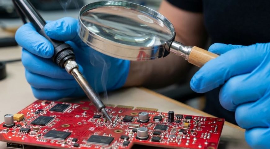
Through-hole soldering using manual methods also requires proper training, especially with lead-free solder, as it has a much higher melting point. Without adequate training, a novice can very quickly ruin a flex PCB when manually soldering a component.

Electromechanical and Cable Harness Assembly

The ability to read diagrams and follow assembly instructions is very critical to the successful completion of an electromechanical and cable assembly. Technicians in this area need to be trained to understand the different symbols electrical diagrams use. Cable harness assembly uses colors and numbers for proper identification and orientation, and technicians need training to work efficiently and quickly using the codes on their assembly drawings.

Final Product Assembly and Automated Testing Services

Professional PCB manufacturing companies usually maintain a state-of-the-art manufacturing facility along with a team of technicians, experienced in product assembly and testing. However, this team also requires training since each product is unique, and they must understand the manner in which the different parts come together to make the product function coherently.

Likewise, testing is unique to each product, and the technicians must be capable of being trained in the unique testing process to be followed for each product.

rushpcb uk-01

Component Purchasing Services

Being completely flexible towards the requirements of the customer, printed circuit board manufacturers also offer turnkey projects that involve component purchasing. There is an inherent danger in an untrained person purchasing components from the open market, as there is always a chance of counterfeit parts coming through. Therefore, technicians involved in purchasing components need training to know reliable sources for electronic components, and the means of identifying counterfeit ones.

Complete Turnkey from Design to Finished Product

Professional PCB manufacturing companies such as Rush PCB Inc. guarantee world-class results in the electronic industry. They make this possible by ensuring their factory floor technicians obtain consistent, regular training. Regular training has the advantage that technicians use standardized methods, follow best practices, generate efficiencies, and improve on the specific process on which they are working.

Both printed circuit board assembly companies as well as PCB manufacturing companies need to implement training schedules that are highly standardized for guaranteeing the top-quality service their clients demand. Consistent training schedules ensure professional PCB manufacturers prioritize manufacturability from the very beginning of the design process.

rush pcb

Rush PCB UK

Best Practices for Assembly and Fabrication of PCBs

Best Practices for Assembly and Fabrication of PCBs

As an expert manufacturer and PCB assembly company, Rush PCB Inc. uses several best practices when working with industries including aerospace, consumer electronics, automotive, and many more. The best practices involve PCB design, technical aspects, and assembly issues.

Best Practices Start Early

Efficient fabrication of PCBs that high-speed circuitry utilizes is essential to ensuring results for the end user. Often, the design of the PCB layout is not thought of as a proactive step in the process. However, it requires advanced thinking and adherence to important factors to provide designs where the results lead to successful fabrication of PCBs to achieve the desired functionality. Designers need to address the practice of DFM or designing for manufacturing and including extra considerations for demands of high speed circuits early in the design stages of board layout rather than taking them on as an afterthought.

The results of poor layout show up during fabrication, assembly, and later on, as issues related to performance when putting fabricated PCBs to testing or production use. However, at that point of time, redesign or rework can be exponentially more expensive and time-consuming, requiring evaluation of circuit failures and reconfiguration of layouts of prototypes.

Material Handling

Best practices in the assembly process of any PCB assembly company start with material handling of PCBs, solder paste, and SMD components.

PCB Handling

Resin coated foils, prepreg, and core materials are susceptible to damage while handling. They need handling by their edges by operators using clean latex or nitrite gloves. Prepreg needs storing on a flat surface in a cool dry environment, preferably at less than 23°C and lower than 50% relative humidity.

If the room temperature of the PCB assembly services is significantly higher than the storage temperature, the prepreg needs to be acclimatized to the ambient temperature, prior to starting assembly. During acclimatization, the prepreg must remain in its sealed package for the stabilization period to prevent any moisture condensing on it. Any unused prepreg must be returned to their package bags and resealed. Therefore, it is best to package PCBs in brick counts that closely emulate run quantities. Prepregs must not be folded.

Some moisture is inevitably absorbed into the PCB material during the time the fabrication process is completed and start of exposure to the assembly soldering. Removal of this absorbed residual moisture may need baking the PCBs at 105-125°C for 4-6 hours.

Also read:  History of Circuit Boards

Solder Paste Handling

As solder paste is a shelf-life dependent item, it should be put directly into a storage refrigerator of the PCB assembly services on delivery, and stored as FIFO or first in first out manner, preferably with refrigerator temperature below 10°C. Preferably store solder past in lots, and ensure older lots are used first for optimal material management.

Manufacturers usually print the manufacturing date on each label and include a use by date for best performance of PCB assembly in UK. This must be strictly followed. Prior to use, equilibrate the solder paste to the environmental conditions where it will be used. For a jar or cartridge of solder paste, it is best to remove from refrigeration one day prior to use. This allows the solder paste plenty of time to equilibrate in the environment. However, this is not recommended for syringes.

Never expose solder paste to heat greater than 25°C for bringing it up to temperature fast. However, temperature-controlled water bath at around 25°C may be used. Whenever removing a container from refrigeration, label it with the date of removal for monitoring exposure.

Although homogenizing solder paste prior to use may not always be required, if necessary, stirring with a plastic spatula is recommended. Solder paste removed from the stencil must always be stored in a separate jar, rather than reintroducing it into fresh paste, as this can result in process inconsistency. Do not return solder paste to the refrigerator after opening the container, as this can cause condensation and compromise performance.

SMD Components Handling

While storing SMD components, it is essential to ensure they are kept in conditions that prevent moisture ingress and avoid electrostatic charge build up to prevent any damage.

While storing incoming SMD material, PCB assembly in UK such as Rush PCB Inc., use an ERP system help to keep track of information such as delivery date, order number, and material data. If unused material is returned to the stores, the ERP system can keep track of the used components, rejections, and damaged SMDs.

pcb

Best Practices for Screen Printing

Consistent stencil printing requires proper board support, typically provided bch as y vacuum tooling. Adequate paste must be used to enable a generous bead to roll freely when the squeegee moves. The squeegee pressure must be adequate to ensure a clean sweep without leaving paste on the stencil after a pass.

Enable proper gasketing to align the apertures with the pads properly. Ensure levelness of the board surface, and solder mask definition must not detract from contact between the stencil and the surface of the board.

Occasionally wipe the underside of the stencil to remove any excess paste. Although wipe frequency is recommended with the product data sheet, it also depends on the process optimization and proper gasketing.

Read Also;   Assembling Wearable Electronics

Best Practices for Reflow Soldering

For best results, the reflow soldering profile should be broken down into four phases—preheat, pre-reflow, reflow, and cooling.

The preheat phase allows preconditioning the PCB assembly prior to the actual reflow. It removes flux volatiles while reducing thermal shock to the assembly.

The pre-reflow phase uses the flux activator to remove any existing surface oxide from the PCB pad finishes, component leads, and any oxides on the powder particles within the solder paste. Basically, it prepares the surfaces to be joined during reflow. This phase also involves a temperature soak, allowing the thermal gradient across the PCB assembly to equilibrate prior to reflow.

The actual reflow of the solder alloy allows the creation of a suitable electrical and mechanical bond. Formation of an optimum bond involves two critical parameters—the peak temperature, generally 20-30°C above the liquidus temperature of the alloy, and the time-above-liquidus, typically 30-90 seconds to form the effective intermetallics.

To form a reliable mechanical bond, the grain structure should be fine, which can be formed via the cooling phase. A rapid cooling rate while transitioning from liquidus to solidus can stress the joint; therefore, a cooling rate of 4°C/second is preferable.

Best Practices for Handling PCB Assemblies

ESD is one of the major causes of failure of assembled PCBs. Therefor proper electrical grounding of worktables and operators is necessary. Worktables must have electrically conducting mats and workers must wear anti-static clothing, while being grounded with discharge straps on the wrists or ankles.

rush pcb