Calculate PCB Trace Width

How to Calculate PCB Trace Width

IPC 2152 vs. IPC 2221: Choosing a PCB Trace Width Calculator

There are two PCB trace width calculators available in the market — one based on graphs published by IPC 2221, and the other based on graphs published by the latest IPC 2152 standards.

The calculator (https://ninja-calc.mbedded.ninja/calculators/electronics/pcb-design/track-current-ipc2152) or (https://twcalculator.app.protoexpress.com/) based on the latest IPC 2152 standards is more accurate and requires more data input. However, for general-purpose use, the calculator based on IPC 2221 is also helpful.

Both calculators find the minimum PCB track width for a specified continuous current and temperature rise. The calculations take into consideration the thickness of the copper track, its distance from planes, the entire thickness of the board, and the material the PCB uses.

IPC 2152 provides graphs, and the trace width calculator uses equations from the data extracted from these graphs. For this, the designers used the tool WebPlotDigitizer, with which they fitted suitable trend lines to the graphs.

The accuracy of the calculator based on the graphs provided by IPC 2152 is quite high, as long as the range of data lies within that provided by these graphs. Beyond this range, the equations tend to extrapolate, but the results can be inaccurate.

The calculator assumes the current to be DC and, hence, constant. However, it is also possible to use the RMS value for a pulsed current, provided the pulses are fast enough.

All PCB materials have a relative thermal index or RTI, and the designer must take care to never exceed the temperature of the PCB material beyond this RTI. The Underwriter Laboratories define this RTI as the temperature at which it is possible to retain at least 50% of the material properties of the material after 100,000 hours. However, this calculator will not take into account heat sources that are active nearby.

Details of Trace Width Calculator Based on IPC 2152

The calculator is basically a three-in-one calculator. The three parameters involved in the calculation are — trace width, maximum allowed temperature rise above the ambient, and maximum current capacity of the trace. Out the three, if the designer knows any two, the trace width calculator can calculate the third.

Additionally, the calculator also provides the DC resistance and the voltage drop across the trace for a given length. 

Expectations from the Trace Width Calculator

Trace width calculations are always critical for PCBs carrying high currents. Therefore, the designer must know the trace width that is just enough for carrying that high current. For instance, if the trace width is not adequate, the current flow may burn out the trace, and impact the functionality of the PCB.

With the trace width calculator, the designer can calculate only the trace width, but also the temperature rise and the amount of current the trace can handle. By altering any two of these parameters, the designer can find out the effect they have on the third parameter. 

As the calculator is based on the IPC 2152 graphs, the calculator provides the temperature rise in not only external traces (on the external surfaces of PCBs), but also in internal traces (buried in the internal layers of multi-layer PCBs).

For instance, the calculator shows that internal traces can also carry quite high currents similar to those external traces can carry. Convection air flow on external traces keep them cooler, and hence, they can carry higher currents. The trace width calculator allows change of units as necessary by the designer.

Using the Trace Width Calculator

While designing traces on a PCB, designers essentially consider four main parameters:

  • Trace Width (W)
  • Rise in temperature (ΔT)
  • Maximum Trace Current (Imax)
  • Trace Thickness (Th)

If the designer knows the Imax and ΔT, then the trace width calculator can provide the trace width for both internal and external traces.

The tool requires ambient temperature input and the trace length also. With these extra inputs, the tool can calculate additional parameters such as trace resistance at ambient and at elevated temperature, maximum voltage drop, and maximum power loss.

Conclusion

The trace width calculator based on IPC 2152 is a versatile tool for PCB designers. They can use it in multiple ways to calculate various parameters of a PCB trace under different operating conditions.

Shorts on Printed Circuit Boards

Detecting Shorts on Printed Circuit Boards

Detecting Shorts in PCBs

It is not an uncommon experience for engineers to find that their newly assembled printed circuit board has a short. Not only does a short prevent the board from functioning as intended, but it may also lead to an uncontrolled current consumption, leading to damage to a few components or to the tracks on the board. According to Rush PCB Ltd, it is necessary to have an understanding of the cause of shorts in PCBs to know how to detect them. Shorts may appear in bare boards and in assembled boards.

Cause of Shorts in Bare Printed Circuit Boards

Lack of proper reviews and inspection methods is the major cause of shorts in bare printed circuit boards. This usually happens due to:

Design issues

While laying out the traces during the design phase, a designer may overlook maintaining the minimum distance between two traces, a trace and a pad, and between two pads. This may be due to inadequate applications of Design Rules and subsequent slip-ups in DFM reviews.

Inadequate etching controls

Inadequate etching may result in copper slivers remaining between adjacent copper instances on the PCB. A proper inspection regime should be enough to detect such deficiencies and adjust the process controls to overcome them.

Cause of Shorts in Printed Circuit Board Assemblies

Shorts may appear in a PCB assembly, even when the bare board did not have any. There may be several reasons for such shorts to occur:

Solder Shorts

Presence of excess solder is the most common reason for shorts. Extra solder bridging two neighboring pads can cause a short. Manual soldering is one of the major reasons for deposition of excess solder leading to shorting between adjacent pins. Another reason is excess solder paste deposition through a thick stencil.

Component Shorts

Neighboring components with metallic bodies may touch each other to cause a short. This is common in boards with through hole components, where components standing out on board is a regular affair, but it is rare with surface mount components.

A damaged component may also be the source of a short. If the component has developed an internal short, it may not be visible externally. However, once the board assembly is powered up, the components acts like a short.

Detecting Shorts in Bare Printed Circuit Boards

Manual Methods

Using a multimeter is an adequate arrangement for detecting shorts in bare PCBs manually. The inspector requires a knowledge of the various individual nets on the board. Test pads provided by the designer makes the testing easier.

The multimeter must show high resistance between any two nets. Any indication of low resistance is due to an unwanted short.

Automated Methods

For quick detection during high volumes of production, automated methods are preferable. Test pins or flying leads touch test pads and assess the resistance between them. A computer compares the readings collected with reference readings from a known good board, highlighting the differences.

Detecting Shorts in Printed Circuit Board Assemblies

Detecting shorts in assembled PCBs is more complicated, and requires the inspector to have experience and ingenuity. Testing for shorts in assembled circuits requires powering the assembly, typically through a current limited power supply, to avoid damaging components.

Depending on the nature of the short, it may be possible to detect it using visual methods or through instruments.

Visual Inspection

If a short circuit is causing a rise in temperature somewhere, it may be easy to spot visually or by touch. The temperature of a trace going up due to a short may discolor the trace, making it easy to locate. A solder short on two adjacent pins of a component may cause a rise in the temperature of the component. Touching components with a finger may help in detecting the hot component.

Thermal Imaging

A thermal image of an assembled board after power-up can give a clue to the presence of a short. Automated devices can compare the thermal image of the test board to that of a reference board, thereby flagging any discrepancies.

Damaged Component

A component with an internal damage may deteriorate when the board is powered up. This may result in visible signs like a bulging capacitor can, a discolored resistor, or flaking colors giving an indication of the fault.

Conclusion

There are various ways a short may manifest itself in a printed circuit board, depending on whether the board is bare or assembled. Detecting the short or shorts quickly depends on the nature of the short and the methods used by the inspector. Rush PCB Ltd recommends understanding the effects of the short to lead to a quick detection.

Standard PCB Board Panel Sizes

Standard PCB Board Panel Sizes

Choosing Optimal PCB Panel Sizes for Cost-Effective Manufacturing

Rush PCB UK uses the latest technologies for making PCBs. Although the production processes for making PCBs are not always easy, we automate most of them. For this, we use special software for parts of the work, especially when we produce PCBs in large quantities. For those new to the world of printed circuit boards, we would like to explain things crucial about PCB manufacturing like standard PCB panel sizes, and why Rush PCB UK is one of the best companies from where to get your printed circuit boards.

Why PCB Panels?

Our customers have their own reasons of getting their PCB made. These reasons are extremely diverse, and the same is true for the myriad sizes of PCBs in the market. Rather than fabricate boards of various sizes, manufacturers prefer to standardize them by designing them in panels.

Once the designer has made a custom printed circuit board, they put them in standard panels. This depends on the manufacturer, as they decide the panel size most suitable to them for optimizing the output, reducing the cost, and improving the quality of the board.

Manufacturers use different methods for depaneling or removing individual boards from the panel. Some use the V-groove method, while others use the tab routing method. The method of depaneling depends on the design of the PCB, and the manufacturer chooses the method that causes the least damage to the boards when removing them from the panel.

Standard PCB Board Panel Sizes

Deciding the PCB Board Panel Size

Another factor that plays a major role in deciding the panel size is the thickness of the PCB. The thickness of a board depends on its application—thicker boards are necessary when it is known that they will be subject to high amounts of vibration, while thin and flexible boards are useful where they will be subject to flexing and bending.

Typically, an average circuit board is 0.063 inches (63 Mils, 1.6 mm) thick. For achieving the highest quality, manufacturers take into consideration the board thickness while deciding the processes for fabrication. They calculate the panel size accordingly so that the area utilization is maximum.

Apart from the size and thickness of individual boards, the panel size also depends on the method of depanelng or separating the individual boards from the panel. This is because the method the manufacturer will use for depaneling decides the separation and clearance between adjacent boards.

When constructing a printed circuit board, manufacturers choose a standard PCB panel size to make their work faster and more efficient. For a standard panel size of 18 x 24 inches, the border clearance should be a maximum of half inch. However, for PCBs with higher number of layers, the requirement of border clearance also increases. As the number of layers increases, more marks are necessary for handling and alignment, thereby taking up more space in the border clearance.

In a board measuring 12 x 18 inches, the layout likely takes up 10 x 16 inches. However, multi-layered boards require additional assembly and marking clearance. Additionally, panels require border clearance, specific routing, and milling clearance. If all the boards in the panel are similar, the paneling is faster, and it costs less. However, if the individual boards in the panel are all different, the paneling process becomes a challenge, and requires experience and skilled professional engineers.

For identical boards, the configuration and paneling process is straight forward, as the process is geometrically identical, and it is possible to automate it by a step-and-repeat process. However, for individually different boards, this strategy fails, and positioning the boards requires an expert to do it manually.

Recommendations for Standard PCB Board Panel Sizes

Rush PCB UK recommends customers to discuss their board requirements with us before placing orders. We cooperate with our customers and try to minimize the board cost while still getting the best possible size.

Economizing the space on the standard PCB panel leads to a reduction in the cost of producing custom circuit boards. Therefore, it is necessary to discuss with us when you happen to decide on the size of your circuit board. We will guide you to resize your board such that panelization works out in the best possible manner.

Conclusion

It is very important that you select an experienced PCB manufacturing company like Rush PCB UK to get your boards fabricated. When you want a high-quality product, there will be several manufacturers who can produce PCBs for you. For us at Rush PCB UK, this is not a problem at all. We not only advise you as to the most optimum size of your PCB, but also inform you about details like dimensions of the space between individual boards and the space around the panel edges.

SMD Stencil and Laser Stencil

SMD Stencil and Laser Stencil

Laser-Cut SMD Stencils for Precise Soldering

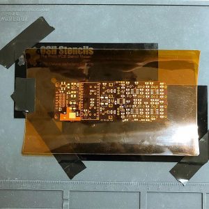
For assembling surface mount devices or SMDs on a PCB, assemblers require a stencil. They use the stencil as a guide to depositing the correct amount of solder paste on the footprint pads on a circuit board. Rush PCB UK recommends using laser-cut stencils to achieve high-quality soldering.

SMD Stencils

Most SMD stencils are made of thin stainless steel foils with openings for the solder paste to pass through. The operator places the stencil on the board and registers the openings to match with the component pads. They apply a small amount of solder paste on the stencil and drag it across with a metal squeegee. The solder paste passes through the openings in the stencil and deposits on the pads on the board.

Laser Stencils

To cut the openings in the stencil accurately, manufacturers use laser beams. The tiny beam of a laser is smaller than any metal tool, and therefore, can make more accurate cuts. Electro-polishing the edges of the cut make them smooth enough to release the solder paste easily.

Most laser stencils are made of stainless steel, although nickel stencils are also available. Manufacturers make the openings in the stencil using lasers. Using laser has the advantage of achieving high precision and low processing time, as there are no photo films involved. The apertures in the stencil are highly accurate when cut with lasers.

Even when cut with high-precision lasers, the walls of the apertures usually have tiny burs. These hamper the smooth transfer of solder paste from the stencil to the board. A process of electro-polishing or nickel plating removes the tiny burs, improving the transfer of solder paste.

SMD Stencil and Laser Stencil

Stencil Thickness

The amount of solder paste deposit required on the pads defines the stencil thickness. SMD stencils are typically 0.006 to 0.010 inches thick. The thickness of the stencil is important to achieve quality solder joints.

If the SMD stencil is thicker than necessary, it will deposit a high volume of solder paste. During reflow, this may cause problems for fine pitch SMDs, as the excess solder may join to create shorts. On the other hand, the high volume of solder paste may also make it stick to the edges of the opening on the stencil, affecting its transfer efficiency, and subsequent transfers. if the stencil is thin, the solder paste it deposits may not be enough to properly form a proper solder joint.

Stencil Aperture

To improve the transfer efficiency of SMD stencils, manufacturers follow stencil aperture rules. Ideally, the amount of solder paste held in the opening of a stencil should transfer totally and completely to the pad, after the operator lifts the stencil. However, this does not happen in reality. A small amount of solder paste sticks to the stencil opening walls. The ratio of the solder paste volume deposited by the stencil to the calculated volume is the transfer efficiency of the stencil, and should ideally be 1 for a specific stencil.

Stencil manufacturers follow a mathematical relationship between the stencil thickness and the stencil opening, to maximize the transfer efficiency. The aperture is usually trapezoidal, such that the bottom opening is wider than the opening at the top of the stencil. This helps to increase the transfer efficiency.

Care of Stencils

After using a stencil, the operator must thoroughly clean it to get rid of any remaining solder paste. Rush PCB UK recommends storing stencils vertically in a suitably protective environment.

Electrical Breadboard

Using the Electrical Breadboard

Breadboards in Electronics: A Primer for Circuit Prototyping

When working on a new project, electronic engineers prefer to test their circuits on a prototype board. This is a printed circuit board on which they mount electronic components and test the circuit functionally. If necessary, they make the necessary changes in the circuit and the layout of the board. Once the changes are satisfactory, the circuit proceeds to the final design. However, even before they go for a prototype board, the designers can do some preliminary testing with electronic components. Rush PCB UK recommends using the electrical breadboard for this purpose.

What is an Electrical Breadboard?

An electrical breadboard is a rectangular plastic board with numerous holes on its top surface. The holes allow plugging in the leads of through-hole electronic components. This allows for building prototype circuits and testing them without soldering the component leads. Unfortunately, it is not possible to use surface mount components with electrical breadboards. Therefore, designers test their circuits using through-hole components and move over to using surface mount components when going for prototype PCBs.

The name breadboard is a leftover from early days of electronics, when people would use nails and screws driven into wooden boards to connect components. As the boards were initially meant for cutting bread, the name stuck.

Structure of Breadboards

The modern breadboard is made of plastic, and is available in various shapes, sizes, and colors. Most common are the full size, half size, and mini size of breadboards. Most breadboards come with notches and tabs on their sides. This allows snapping more boards together to build one large breadboard.

Electrical Breadboard

Figure 1: Electrical Breadboard

A full size breadboard has its holes arranged in rows and columns. The longer sides have two rows of holes each, and the arrangement of 30 columns are in two groups, A to E and F to J.

The breadboard does not require soldering components to connect them. Under the board, each hole has a brass connector with spring leaves. When the designer pushes the lead of a component through a hole, the spring leaves of the connector anchor it securely. The design of the spring leaves is such that it is easy to pull out the lead and plug it into another hole.

The interconnection between the brass connectors makes the breadboard so convenient for building circuits. The two rows along the longer side of the board have the connectors joined individually. Therefore, the designer can use them as power buses. They can designate the outermost rows on the two longer sides as the ground or the negative bus and the rows immediately on the inner side as the positive bus of a DC power supply.

Likewise, the two groups of 30 columns also have their connectors interconnected individually. However, there is no interconnection between the two groups. They are also isolated from the power buses.

Using the Breadboard

The design of the breadboard is such that the rows E and F have a separation of 0.25 inches between them. This allows placing an IC such that it straddles the rows E and F. Each pin of the IC is then extended by four connections. The designer can plug in resistors, capacitors, and other components between the pins of the IC. They can make other electrical connections with the help of wire jumpers.

Using the Breadboard

Img Source: https://cdn.sparkfun.com/assets/0/3/f/f/1/51758c9ece395fd266000000.jpg

Conclusion

With no special tools necessary to use them, breadboards are a great way to build electronic circuits. As there is no soldering necessary to interconnect components, even newcomers to electronics can experiment with components to build and test circuits. Once they have finalized the circuit and tested it on a breadboard, they can develop a prototype board that Rush PCB UK will gladly fabricate for them.

Read More about: How do Circuit Boards Work?

FR4 Printed Circuit Board

All About FR4 Printed Circuit Board Material

FR4: The Backbone of PCBs for Electronic Engineers

According to Rush PCB UK, FR4 is the most common material that PCB manufacturers use to make printed circuit boards. Most individuals and engineers in the electronic industry are familiar with FR4 as the base material for building rigid circuit boards.

What is FR4?

The name FR4 or FR-4 is a combination of an acronym and a grade. The FR stands for Flame Retardant and the 4 is the mark of a grade of the material. FR4 is an epoxy laminated fiberglass reinforced sheet that printed circuit board manufacturers use. Grade 4 indicates the base quality of the laminate sheet.

Under the FR4 name, there exists a variety of sheet materials and designs, with the number differentiating them from others in the same class.

FR4 has a composite structure. Fiberglass, woven into thin cloth-like sheets, is bound with a flame-resistant epoxy resin, to form a base layer for a printed circuit board. While the fiberglass gives the material its structural stability, the epoxy gives FR4 its material rigidity. FR4 also has several other physical properties that make it so popular among engineers and designers as a base PCB material.

How PCBs Use FR4

The FR4 in a PCB forms its primary insulating backbone. Board manufacturers laminate the FR4 sheet with copper foil on both sides using adhesive and bond them with heat and pressure to form a copper clad. PCB manufacturers use the copper clad to build printed circuit boards. Depending on the design, they etch the copper foils to form circuits on which they solder electronic components.

Complex PCBs can have more than just two layers. Manufacturers etch Inner layers of copper foils to form specific circuits and bond all the layers to form a single multilayered PCB. Vias form the interconnections among the inner and outer copper layers. The outermost copper layers need a covering of solder masks to keep them from being tarnished and oxidized from chemicals in the atmosphere. A silkscreen layer helps in the assembly process.

Depending on the application, designers choose the FR4 and copper foil thicknesses. Unless the board has to withstand severe vibrations, designers use standard thickness FR4 material. The copper foil thickness depends on the current the board must handle.

When to Use FR4

Designers prefer to use FR4-based printed circuit boards for their mechanical strength, reliability, good electrical insulation, and relatively low cost. However, FR4 material is not suitable for boards handling high-frequency signals, which require special laminates for better signal integrity.

PCB Thickness

When ordering a printed circuit board for a project, the designer must specify the number of layers and their thickness. Depending on the needs of the project, the thickness of the FR4 board may vary significantly. This is an essential feature and affects many aspects of the functionality of the board.

Advantages of Using FR4

FR4 materials are popular among electronic engineers in the industry as FR4 offers several advantages:

  • Easy to design and fabricate
  • Low-cost materials
  • Makes compact boards
  • Provides good bonding with copper foils—high peel-off strength
  • High mechanical strength
  • Highly resistant to moisture
  • Good electrical insulating properties in humid environments
  • Can withstand high temperatures
  • Can be fabricated into multiple layers
Properties of PCB Materials

Properties of PCB Materials Ref: https://www.semitracks.com/newsletters/images/august/2015-august-newsletter-image-1.png

Types of FR4 PCBs

Depending on the filler material, it is possible to make various types of FR4 boards such as:

  • Halogen-Free PCBs
  • Single-Layer PCBs
  • Double-Layer PCBs
  • Multi-Layered PCBs
  • Rigid-Flex PCBs

Conclusion

Being a widely relevant material, FR4 is popular mostly for its low cost and relative electrical and mechanical stability. Although FR4 material is popular for its extensive benefits, it is not the best material for high-frequency applications. For any requirements of PCBs made from high-quality FR4 material, please contact Rush PCB UK.

Types of Prototype PCBs

All About Double-Sided Prototype PCBs

Prototype PCBs: Testing Electrical Circuits

Electrical and electronic industries use printed circuit boards or PCBs for various activities and equipment. These boards may be single-, double-, or multi-layered, with copper traces on each layer confirming to certain schematics. PCBs hold the necessary electrical and electronic components in place with solder, allowing easy wiring and assembly. However, before committing to manufacturing PCBs in large numbers, Rush PCB UK recommends designers test their circuits using prototype PCBs.

What are Prototype PCBs

Prototype PCBs are general-purpose boards available off the shelf. Designers typically use these boards to assemble their circuits and test them for their functioning. Once the designer is satisfied the assembly is functioning according to their requirements, they can proceed to the next step towards designing and layout of the actual board.

The structure of the prototype PCBs is such that it is easy to desolder any component and replace it with another. This feature is helpful to designers since it allows them to change components if the circuit does not function as desired.

Types of Prototype PCBs

The structure of prototype PCBs varies depending on the type of components the designer is planning to use in their application. In general, there are two major types, depending on whether the designer is using Through-Hole Components (THCs) or Surface Mount Components (SMCs).

THCs have long leads protruding from the body of the component. The PCB requires holes to allow the component leads to pass through for anchoring and soldering. It is possible to solder the components manually using a soldering iron, or using a wave soldering machine.

SMCs have very short leads that do not require holes for mounting. It is possible to place the SMC on the board and solder the leads directly to the pads on the board. For medium-SMCs, it is possible to manually solder them using a fine-tip soldering iron. However, it is possible to use a table-top reflow machine to solder SMCs on prototype boards.

Double-sided prototype PCBs for THCs

Two popular types of double-sided prototype PCBs are available for use with THCs:

Perf Boards: These are double-sided FR-4 boards with identical patterns. Each perf, or perforated board, has 1 mm holes drilled at 0.1-inch pitch all over it. Each hole has an unconnected square or round copper pad surrounding it. The holes are not plated through. In general, the boards are available in various sizes such as 4 in x 3 in, 6 in x 6 in, 4 in x 8 in, 6 in x 8 in, and so on.

Strip Boards: Similar to perf boards, strip boards are double-sided FR-4, with 1 mm holes drilled at 0.1-inch pitch. While all the holes have square or round copper pads surrounding them, each pad connects to its horizontally adjacent neighboring pad with a copper trace, with the trace running from the left edge of the board to the right edge. The reverse side has a similar circuit, only the trace connections are vertical rather than horizontal, with each trace starting from the top of the board and running to its bottom. Therefore, the board has many parallel strips of copper trace on each side, with the strips running at right angles on the two sides.

Types of Prototype PCBs


Double-Sided Prototype PCBs for SMCs

Two types of double-sided prototype PCBs are available for SMCs:

General Purpose Customizable Boards: These are double-sided FR-4 boards with patterns on both sides. The patterns have pads capable of accepting various SMC sizes for resistors, capacitors, inductors, edge mount connectors, and SMA connectors. These boards are generally available for medium-sized SMCs like 1210, 1206, and 0805.

Several plated through holes (PTH) are available very close to the component pads but not connected to them. These PTHs help the designer to easily connect to the circuit on the other side.

Specific Purpose Boards: These are double-sided FR-4 boards with specific patterns on both sides. The circuit on each side has pads for SMCs arranged in clusters of 4, 5, or 6 components. Designers can use SMCs of 1210, 1206, and 0805 sizes on these boards.

The boards have numerous PTHs placed close to the clusters of SMC pads. These help the designer to allow connection to the circuit on the other side of the board.

Specific Boards for SMC ICs: These are double-sided FR-4 boards with a specific SMC IC pattern on one side of the board, along with pads for discrete SMCs. The IC pattern has only pads for a quad package or dual-in-line package IC. The pads are usually long to allow mounting different-sized packages. All the pads have a neighboring unconnected PTH to allow connection to the reverse side.

How to Use Prototype PCBs

The basic idea of using prototype PCBs is to build a circuit using electronic components and test its functionality. The designer selects the type of prototype board depending on whether the circuit uses THCs or SMCs.

Using Prototype PCBs for THCs

For THCs, designers can use either perf or strip boards. In general, beginners find perf boards or perforated boards easier to use because they can interconnect components using short pieces of wire or even with solder bridges. The leads passing through the holes also double as connections to the other side of the board.

Experienced designers find the strip board more useful, as they can use the strips as interconnections between components. For a short interconnection, they can interrupt the excess strip on either side with a sharp cut.

As most through-hole ICs have a pin pitch of 0.1 inches, placing ICs on the perf, or stripboard is easy. However, the designer must ensure the strips do not short the pins of the IC.

Using Prototype PCBs for SMCs

Using prototype PCBs for SMCs is somewhat different from those for THCs. The complexity arises because of various factors. SMCs are available in various package sizes. SMC ICs can have quad packages or dual-in-line packages and their pins can be in gull-wing, J-wing, or flat shape. Fortunately, most manufacturers offer the same IC in different packages, so the designers can choose accordingly.

Conclusion

Rush PCB UK recommends designers use prototype boards for testing the functionality of their circuits before finalizing their designs. Having to redesign a board results in unnecessary delays and cost overruns, making the design late to the market. Using prototype boards is an easy way for the designer to maintain the schedule according to the plan.

PTH Via

Current Carrying Capacity in PCB Vias

Current Carrying Capacity of PCB Conductors and Vias

The current carrying capacity in PCB conductors is a common question from new designers. According to Rush PCB UK, along with the current carrying capacity of PCB conductors, the current carrying capacity of PCB vias is of equal importance, especially when the design is of a new board that must carry high currents. The designer must keep the conductor and via temperatures below an appropriate limit, and this in turn helps to keep components on the board cold enough.

Although the IPC 2152 standards deal extensively with the recommended current carrying capacity of traces, they focus much less on vias in multi-layered boards. However, there have been several investigations into current carrying capacity and temperature limits, while comparing them to the temperature excursions of typical traces carrying the same current.

Importance of Via Current Carrying Capacity

Designers typically specify the current carrying capacity of traces that will be carrying high current. They usually determine this using the copper weight and the allowable temperature rise, while using the nomograph in the IPC 2152 standards. They aim to size the traces such that the components and the board will remain within safe temperature limits while operating. If there are vias on the traces, it is important to compare the temperature rise in the vias with that of the traces and or planes to which they connect.

PTH Via

Figure 1: Various Types of PCB Vias

As the via connects, at each end, to a hot trace that is carrying a high current, it is reasonable to expect the via temperature to be at least as high as that of the traces that connect to it. Planes and traces connected to the via can get quite hot with the passage of high currents, especially for low copper weights carrying 5-10 Amperes. Therefore, it is natural to expect heat accumulation in vias. Also, with exposure to air for traces on the surface layers, it is natural to expect they will run cooler compared to traces buried in the interior layers of the board. These are significant considerations that relate to the via reliability, especially for microvias.

In reality, the situation is contrary to popular intuition. Traces on the surface run at temperatures higher than that of buried traces in internal layers. At 25 ℃, the thermal conductivity of air is approximately 0.026 W/mK, while that of FR-4 is about 0.25 W/mK. In addition, alternative substrate options are available that offer even higher thermal conductivity. That means the substrate acts more like a heat sink for conductors passing through it. As the substrate also surrounds vias, the above applies to vias as well.  This helps to explain the fact that vias tend to have a lower temperature compared to traces that connect to them. An article in the Signal Integrity journal, by Douglas Brooks and Johannes Adam, substantiates the above through measurements and results.

Read About: Make Your PCBs More Reliable with Vias

Rule of Thumb

Engineers often prefer to follow the 0.5 A rule of thumb. As this rule offers a conservative result, it is acceptable to follow in most cases. However, for higher DC currents, an excessive number of vias may do more harm than good when the designer is connecting them to planes. For instance, the designer may have set a limit of 1 A per via. If they must supply 5 A instantaneously, they can safely place 5 large vias with thick plating, as long as the via temperature is not too high near a component.

In practice, the danger in the above example is not about the high temperature in the vias. Rather, it is more about temperature cycling. If the temperature swings between very low and very high temperatures, it might lead to fatigue setting in, resulting in failure.

Analysis of Current Carrying Capacity of Vias

In practice, thin traces on outer layers exposed to air and carrying high currents often operate at higher temperatures as compared to the temperature of vias connecting to them, although the difference is only a few degrees. This is due to the thermal conductivity of air being lower than the thermal conductivity of the substrate material surrounding the via. The net effect is the via loses heat faster than the thin traces can dissipate it into air.

While the above is true for thin traces, the situation reverses itself for wider traces. For instance, traces with widths of 200 mils and above can operate at temperatures lower than that of connected vias, although, the temperature difference is only a few degrees. This is because the heat loss from the wide trace now has two components. While the trace loses heat to the surrounding air, it also loses heat through the higher thermal conductivity of the substrate in contact with it. As the heat loss depends on surface area, and the trace is wide, the exposure is now through a much larger surface area of the trace. This allows a wide trace to have a lower temperature at equilibrium. Therefore, it is safe to summarize as follows:

  • For thin traces, vias act as heat sinks for the trace
  • For wide traces, the trace acts as a heat sink for the via

Of course, there are additional factors in the above analysis—the contribution from planes in layers. In reality, large planes act as additional heat sinks, further lowering the operating temperature of the conductors. Moreover, the designer can use alternative substrates with even higher thermal conductivity than that of FR-4. This removes more heat from conductors and vias, leading to an even lower temperature at equilibrium.

Deciding on Via Size

The designer must size the conductors according to the IPC 2152 standard guidelines for carrying high currents. They must also provide thick-walled vias. As the temperature of the via will not rise above that of its conductor, the design will not require further considerations related to vias.

The heat from the via will dissipate into the substrate and the nearby planes and traces. If the traces already have wide surfaces, they will dissipate more heat from their larger surfaces as compared to that dissipated by the via. Therefore, as the heat leaves the traces faster than it does from the via, the entire system will operate at a lower equilibrium temperature.

The current carrying capacity of the via also depends on its thermal conductivity, which the designer can control by adjusting the copper weight, thickness of the prepreg material, and/or the material filling the via.

Conclusion

Rush PCB UK recommends using a reputed PCB CAD design software that allows creating professional via designs and building a stackup from a wide variety of standard substrates.

PCB Board

All About PCB Testing Methods

PCB Testing Methods: Ensuring Quality and Reliability

At Rush PCB UK, we ensure all printed circuit boards for our customers are fully functional before delivery—as the consequences of failure are pricey. We are as concerned as the customer is about non-functional PCBs because of a QA or a design issue causing a shortened life span.

For us, testing PCBs during assembly is an integral part of our manufacturing process. As a reputable electronics contract manufacturer, we offer a variety of PCB testing methods, to make sure all our boards are dependable and of high quality. To let our customers know the PCB testing methods we use, here is a short primer.

Automated Optical Inspection or AOI

AOI methods of testing typically use a single 2-D camera or two cameras for a 3-D photo of the PCB. A computer program compares the photos of the board to a detailed reference photo. If the photo does not match the reference photo to a certain degree, the program flags the board for inspection by a technician.

AOI methods are useful for detecting issues early in the manufacturing stage. We use AOI methods at various stages of manufacturing—after solder paste deposition, after component placement, and after reflow soldering. However, as the test does not require powering up the board, it is not a completely foolproof method.

Automated X-ray inspection or AXI

X-ray testing is necessary for inspecting parts of the PCB that may not be visible under normal conditions. This includes soldering under BGA and similar ICs and internal PCB layers. BGA and similar ICs hide solder joints underneath the chip package. However, X-ray inspection methods require trained and experienced operators. Also, not all the PCB can be examined or inspected using X-ray methods, but it is possible to view:

  • Hidden Solder Joints
  • Traces on Internal Layers
  • Barrels of Plated-Through-Holes
  • AXI tests can be 2-D or 3-D, with the latter offering faster testing.

While we restrict the above two testing methods primarily to assembly processes, we use other testing methods after completing the PCB assembly.

In-Circuit Testing

One of the most robust PCB testing methods, its cost depends on the board and type of fixture necessary. In-circuit testing is also known as bed-of-nails testing, as the fixture we use has several probes protruding from a test bed. We place the board on these probes and power it up. The layout of the probes matches the design of the board,

The probes check the integrity of the solder connections. A computer program measures various parameters using the probes and compares the readings with a reference chart. Any mismatch raises a flag for further inspection by a technician.

Flying Probe Testing

This method is a variation of the in-circuit testing method with the difference that no fixture is necessary. Also, during the testing with flying probes, it is not necessary to power up the board. As there is no fixture necessary, this testing is less expensive as compared to in-circuit testing.

A computerized program allows two or three probes to connect to different parts of the board for testing various parameters like:

  • Shorts
  • Opens
  • Resistance
  • Capacitance
  • Inductance
  • Diode functions

Similar to the in-circuit testing method, the computer compares the results of the flying probe tests to a reference chart. Any mismatch raises a flag for further inspection by a technician.

Functional Testing

This test requires the board to be powered up. A test jig or fixture records various parameters of the board, and a computer compares the results to a reference chart. Inspection by a technician is necessary if there is any mismatch.

Burn-In Testing

This is a more intense form of testing for PCBs that have passed the above tests. This test detects early failures and establishes a load capacity. We power up the board to its maximum specified capacity and allow it to operate continuously for a specified number of hours. This test weeds outboards with high infant mortality rates.

Conclusion

As all tests carry a cost factor, we always consult our customers before setting up a testing scheme for boards. However, we always perform automated optical inspection and automated X-ray inspection (if necessary) during the assembly processes to ensure high quality.

pcb printed circuit board

UK’s Leading Custom PCB and Electronic Board Manufacturer

Superior Turn-Key Custom PCB Solutions & Prototyping

Our mission at Rush PCB UK is to provide our customers in UK and Europe with a superior turn-key custom PCB and assembly solution. We have in place Quality Management Systems that rival those of large-scale manufacturers, and we can build PCB electronic assemblies for our customers that exceed the exacting standards they demand. At the same time, our commitment to personalized service makes us more responsive to our customer’s needs, enabling us to complete our electronic custom build quickly and accurately.

Our customers come from a wide range of industries—from semiconductor production equipment to electronic vehicle manufacturers to medical equipment manufacturers—and we cater to a wide range of technologies. We offer specialized prototyping services in addition to several other solutions, allowing us to meet the customers’ PCBA needs with the quickest turnaround in the industry. Our end-to-end custom circuit boards solutions consist of:

  • Engineering and Design
  • Electronic Circuit Board Manufacturing and Testing
  • Custom Prototyping

UK’s Leading Custom PCB and Electronic Board Manufacturer

End-to-End Custom PCB Solutions

Whether our customers need accurate turn-key fabrication or the highest quality build of a rapid prototype, our expertise remains unparalleled. With more than two decades in the industry, we at Rush PCB UK know how best to build and assemble custom printed circuit boards, PCB electronic assemblies, and box builds that meet and exceed our customers’ needs.

We staff our engineering department with industry experts who fine-tune our manufacturing and testing processes for precision. We are certified for ISO 9001 and ISO 13485, and our products comply with UL 508A and IPC 610. All this allows us to claim the technical proficiency necessary for designing our customers’ electronic circuit boards.

Engineering and Design

Before we take up a project, our engineering team evaluates the data and documentation submitted by our customers. Our engineers specialize in DFM, DFA, and DFT, and apply these methodologies to ensure the project will proceed with the minimum potential issues. We review our customers’ designs for manufacturability and testability and work closely with the customer to resolve all potential issues. If necessary, we have the expertise to redesign the electronic circuit boards for our customers.

Electronic Circuit Board Manufacturing and Testing

At Rush PCB UK, we lead the industry in electronic circuit board manufacturing and assembly—we deliver the best results in the shortest possible time. We include expert engineering insights with our end-to-end custom circuit boards solutions, regardless of whether we are manufacturing PCB electronic boards for a production run or for a prototype.

Custom Prototyping

Our customers often require a prototype custom PCB for their proof-of-concept design, and usually, their requirement is urgent. To handle such custom prototyping projects, Rush PCB UK has an entirely separate team specializing in building prototypes. Our dedicated prototyping team uses a fast-tracked, limited run, quick turnaround manufacturing process to complete the custom PCB design in the shortest possible period.

For such fast custom PCB prototypes, we assign a product specialist to fast-track all the production steps. We immediately procure the parts, fabricate the custom PCB in-house, and the next day, the custom circuit board is ready for assembly.

In the meantime, out engineering staff starts work with the customer to resolve any potential design and manufacturing issues. Our product specialist evaluates the design throughout the entire manufacturing process, ensures completion of the board assembly, and ships to the customer as quickly as possible. This allows the customer to continue with their product development.

Conclusion

We, at Rush PCB UK, have a proven track record of working closely with our customers in UK and Europe as partners for rolling out new products into production and for providing them with proof-of-concept custom electronic circuit boards. Apart from our custom PCB manufacturing services, our fully staffed engineering department also works proactively with our customers in ensuring the successful manufacturing of a robust and repeatable design. We offer specialized prototyping services along with a host of other solutions. That enables the quickest turnaround to meet the PCB electronics needs of our customers.