Choosing a PCB Manufacturer

Things to Consider when Choosing a PCB Manufacturer

Choosing the Right PCB Manufacturer for Your Gizmo: Key Considerations

Your organization has realized that there is a need for a new form of gizmo. You’ve come up with the concept for the gizmo, and realize that a pivotal part of making the gizmo work is having an effective circuit board. The board is in the concept stage and now you’re ready to move into production.

An internet search to find manufacturers for your boards found 237 possible suppliers. How do you choose which one to go with? Considering the following points should make your decision easier.

1) Will you need a prototype?

A prototype can be an important part of PCB development. It lets you test the functionality of your gizmo. It will be much easier to make minor adjustments or major design changes based on the effectiveness of the prototype. Once you are confident that the prototype is functioning as expected, full production can commence. Ask yourself:

  1. Do you need to make a prototype stage; and
  2. Do the manufacturers you’re considering have the scope to print prototypes?

The response will help narrow down the range of manufacturers being considered.

2) Will your production run be low or high volume?

As a guide, low volume production is likely to be about 100 boards per year.  High volume production can be more than 1,000 boards per month. A high volume manufacturer is unlikely to want to break their production run for a small job. Conversely, a manufacturer that focuses on small print projects may not want to be burned with a large production run. Some manufacturers can provide both services.

3) Where should your supplier be based?

There are likely to be three choices:

  1. Local
  2. Domestic
  3. International

You can meet with a local manufacturer, face-to-face, and you can work hand-in-hand with them in development and production. While this may be an advantage, it should be weighed up against the other factors being considered.

There are many good domestic manufacturers. Communication will be within your time zone (give or take), and courier services will help ensure you can conduct your product tests within a relatively short time from printing.

Overseas manufacturers can deliver high quality PCBs, and may be more cost effective than domestic providers. The trade-offs includes subject to international freight and logistics, the risk of exchange rate fluctuations and language barriers.  Time zones may also affect communication.

4) Time Frame

The old truism in manufacturing is that customers can have any two of: Quality, Price and Timeliness. If you’re prepared to trade off timeliness to ensure cost effectiveness and quality, then make that choice early in your decision making process.

As you work through potential suppliers, ask them about the timeframes they need to work in to deliver boards for your gizmo. It is far better to know the timeframe before committing to a manufacturer than to commit, and find out later that their time frames don’t align with your expectations.

 5) Special Requirements

Your design may include special requirements like material, thickness, the number of layers, or the hole sizes. Not all manufacturers can deliver against these special requirements. You will need to confirm the capability of potential manufacturers to meet any such special requirements.
tested pcb

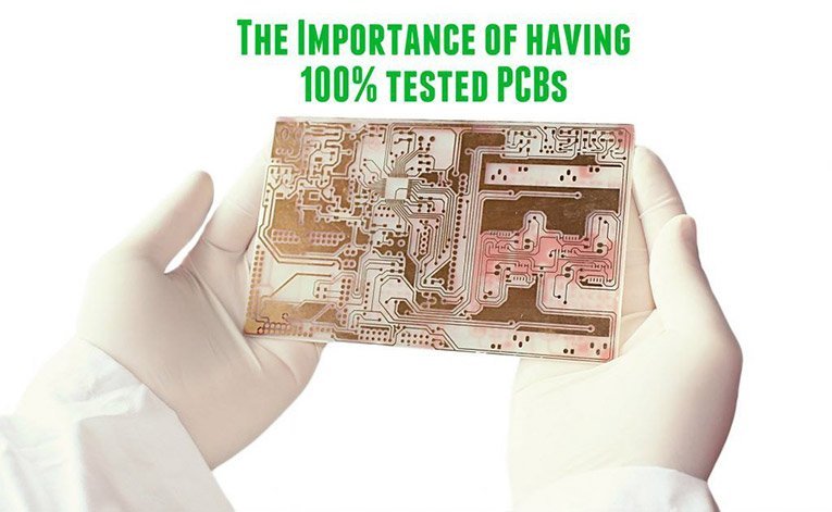
The Importance of having 100% tested PCBs

Importance of 100% Testing in PCB Manufacturing for Quality Assurance

If you’re looking to buy printed circuit boards (PCBs), it will always be worthwhile to ensure your boards have been 100% tested. If you search online for reasons that a PCB doesn’t work, you will find that there are several reasons; any of which may be challenging to troubleshoot. It is a far more worthwhile option to have your boards tested 100% before problems arise.

Think of it this way – a board that has been tested 100% will give buyers confidence about the quality, reliability, and durability of the product. Some reasons that purchases should only be made from manufacturers that 100% test their boards include:

Verifying the Prototype

When boards are being designed, prototypes should always be made. These prototypes are a trial of the final PCB, manufactured on short runs. The designer will test the prototype on an iterative basis to ensure it meets all the design specifications and intended outcomes before commissioning the printing. Once all the details of the board meet the specifications, the designer will have confidence in manufacturing.

While the process of printing and testing prototypes can be expensive and time-consuming, there is significant value in ensuring that the PCBs are error-free before full production. There are a range of issues that can be identified through this testing process such as reversing polarity, identifying shorts, and identifying any missing components.

Automated Optical Inspection

Automated optical inspection (AOI) is the automated visual inspection of PCBs. A camera will scan the PCB to identify issues such as missing components and quality defects. The digital image recorded by the camera is compared to the original design of the PCB. If there are any differences, they can be corrected before printing.

As AOI is a non-contact test method, it can be used at various stages of PCB manufacture. The same board can undergo AOI as a bare board, when the solder paste is in place, pre- and post-reflow. AOI will make sure that the layers are properly constructed before the board is laminated.

X-ray Inspection

Automated X-ray inspection (AXI) uses X-rays to automatically inspect features that may be hidden from view. As with AOI, the goals of AXI are to optimize processes and to detect anomalies. X-ray inspection can reveal the smallest defects in a PCB. This is especially true of defects that may be covered by other components. Faults that can be identified include components not properly fitting, internal cracks, problems in lamination, and porosity issues. Using X-rays is invaluable, as the testing can easily identify defects, allowing the designer to fix them before production.

Functionality Testing

The functionality test is usually the final test before production. Trained quality control engineers test the circuit board to identify if the components are functioning correctly; and if the PCB is producing the expected outcome.

Summary

Quality Control is an essential part of any commercial process. A single PCB that is released to the market without having been thoroughly checked may impact the reputation of an organization that historically has had an impeccable name in the industry. Even if the board is only one out of thousands (or millions) of PCBs made by the organization, the risk of a poorly performing board going to market is one that is not worth taking.

What Can a Reliable Turnkey Service Do for You

What Can a Reliable Turnkey Service Do for You?

RUSHPCB: Your One-Stop Solution for Turnkey PCB Production and Reordering

When putting together any Printed Circuit Board project, chasing down a design, then your components, and then a company to assemble it all, can be a complete hassle. However, RushPCB offers turnkey production and design services to make your project easier to design and produce, which saves money as well as time.

We have an on-site staff of designers and fabricators who can work with you to put together any product, using the latest techniques and technologies. You can either upload your own BOM design file to our ordering system and have us structure your PCB, or you can work with one of our talented and knowledgeable staff to design a PCB that fits all of your needs. We also have a variety of options when it comes to selecting your components. We have a list of recommended parts distributors, as well as a network of suppliers who can work within most budgets to obtain components that will work for your project, yet are still of the highest possible quality. We also have state-of-the-art on-site equipment for putting together your PCB order. Our on-site capabilities include mixed assembly placement, surface mount technology (SMT) soldering, pin-through-hold soldering, and mixed component assembly soldering (and mixed component assembly). We offer a variety of surface finishes including hot air solder leveled (HASL), gold flashing, carbon ink for keypad application, soft gold, and several other capabilities, depending on the requirements of your project. We can also produce PCBs for military and aerospace projects, Ball Grid arrays, or rework an existing PCB that you might need, and can produce either flex or rigid PCBs. All RushPCB projects are fully tested for functionality and quality control, to ensure that your project is flawless and performs according to your expectations.

Having all of the resources you need in one place means that RushPCB can easily save your order details, including specifications, design, components list, and assembly method.  This allows us to provide full turnkey reorder services, saving you time, and providing you with the PCB projects that you need in less time, and with no guesswork. Your past orders will all be available online in your personalized customer account.  To reorder, you only need to go into your account, select a quantity to reorder and submit your request.  Making changes is easy, too.  Using your past order details, we can make any adjustments to your PCB order that you might require, from simple changes such as changing your order amount, to more complex changes including changing component requests. Our team can easily amend any order in our system, and produce it on-site.

At RushPCB we pride ourselves on producing the best-quality PCBs for our clients, efficiently and cost-effectively, and our ability to provide turnkey production and reordering means that you’ll have your project in your hands, and ready to implement, quickly, whether it might be a brand new order or a continual reorder. We are here to help you with any aspects of your PCB production needs.

IOT

The Internet of Things

The Internet of Things: Connecting Devices for a Smarter Future

Maybe you’ve heard of the Internet of Things. It’s a concept that has been around for many years and is starting to become a reality.

Going back about 20 years, the concept of the internet was new, and the opportunities that the web contained were unproven. Household names such as Facebook, Amazon, and Google didn’t exist at the time. Over the last twenty years, the internet has become a tool for common communication, information, and interaction… between people.

The Internet of Things is another step. Although the term was first used in 1999, it has only come into common use recently. The Internet of Things can best be described as the network of devices that are linked to other devices without the need for human interaction. It is estimated that there are already nearly five million devices connected, and Forbes Magazine suggests that by 2020 there will be over 26 billion devices connected.

Think of the factors that have changed in accessing the internet over the last twenty years. The world moved from dial-up to broadband and then fiber. Remote 4G technology now provides timely access to the internet using tablets and smartphones wherever people are.

At a basic level, people are becoming accustomed to the idea of using the internet to remotely access devices. Some people have home security systems that can be accessed through a website. Others can turn home heating systems on and off remotely using the internet. You can set your Digital TV Recorder to record a program at home using your internet, anywhere. All of these interactions still require human activity. They are examples of using the internet to interact with things.

In continually more situations, devices are being designed to connect, without the need for human interaction. The simplest way to think about it is to realize that any device that can be connected may in the future be connected. This could include your garage door remotely opening as your car approaches it, or your car automatically sending a text message if you’re stuck in slow-moving traffic. Your printer could be programmed to know when it is running low on toner or paper, and automatically place an order with the stationery supplier for replacement stock to be delivered. These linkages all meet personal needs.

In the future, the Internet of Things will have effects on you without you being aware of it. Think of traffic flows being automatically adjusted based on the number of vehicles on the road at any given time. Think of manufacturing processes being automated and linked with suppliers of material to maximize the efficiency of supply and distribution channels. All devices that use electricity can interact with utility companies to balance power generation and usage. Remote health monitors can provide real-time information to medical staff regarding patients in their care. The opportunities for devices to interact with each other to benefit our lives are endless. And over the next few years, these advances will start appearing in our daily lives, probably without us even being aware of the new, efficient Internet of Everything.

RUSHPCB.CO.UK Manufacturer and PCB Assembly – UK

pcb history

The History of PCBs

Evolution of PCBs: From Eisler’s Printing Technique to Modern Miniaturization

For many people today, PCBs are an integral part of life. Many people are never more than a few feet away from a PCB – the TV, the microwave, the computer, the car, the smartphone… and the list goes on. Yet we probably all know someone who was alive before PCBs were invented. Well… maybe not! They have been around for longer than most people think.

Most people trace the origin of the PCB to Paul Eisler. In 1936, this Austrian developed the concept of using a printing technique to lay electronic circuits onto an insulating base. Prior to this, components were hand-soldered. Eisler’s concept was to lay wires down on the board, then add the components over the board. Eisler moved to England to escape the Nazis. There was varied interest in his concept, and it took a further seven years for him to apply for a patent for the circuit board. The patent was eventually granted in 1950.

Eisler wasn’t the first to consider using pre-defined electrical paths. In 1935, Charles Ducas applied for a patent for creating an electrical path on an insulated surface. At this time, boards holding circuitry were made of various non-conducting material (including wood, Bakelite and Masonite). To make the boards function, holes were drilled into the boards, and brass wires were riveted in. Others laid the ground work for Ducas. Albert Hansen, Thomas Edison, Max Shoop and Arthur Berry were all working on the concepts that would morph into PCBs as early as 1903.

In 1943 the United States realised that there was a benefit to the technology, and incorporated Eisler’s boards into proximity fuses. In 1947, the first double-sided (non-printed) board was developed.  By 1948, the US established a standard procedure for all airborne circuitry to be printed.

By the 1950s, circuit boards were moving from being purely military into the commercial world. A range of design changes made the boards more practical. In 1956, a patent was filed for “Process of Assembling Electrical Circuits”. The process involved drawing the wire pattern. This was then photographed onto a zinc plate. The plate was used to create a plate for offset printing.

The 1960s saw a number of advances. Multi-layer boards (4+ layer count) began to be produced. Methods were introduced to stop corrosion. This protected the trace and the components, and kept them cleaner (and therefore more efficient).

Through each generation, the PCBs were progressively becoming smaller. In the 1970s, the issue of bridges forming between pads was addressed through the use of solder masks – a thin layer of polymer applied to the copper, or through liquid photo imageable masks or LPIs. In this process, photo-polymer is coated on the circuit, and then dried at controlled temperatures. Unnecessary solvent is then removed. This process became industry standard.

The 1980s saw a continuation in the miniaturisation process. Surface-mount parts became the preferred design option – previously, through-hole components had been preferred. With the advent of SMT, additional developments were required to make the PCBs effective. Stencil techniques improved, as processes such as laser, electroform and chemically etched plastic stencils were developed. Each of these processes allowed for progression of PCBs.

In the 1990s, computer aided manufacturing (CAM) allowed for PCBs to be designed and tested before being printed. The complexity of PCBs increased. High Density Interconnector PCBs were introduced from around 1995. These boards are reduced in weight and size. They have smaller lines and pads.

An indication of the miniaturization process over time can be seen in the specifications. Historically, the standard sizing was measured in ‘mils’, which is a thousandth of an inch. Through-hole components had pins located at 100 mils. Surface-mount components have a pin pitch of 50 mils. Small Outline Package (SOP) boards have pin spacings of 25 mils. In the 2000s, tracing separation continued to decrease, moving to 5-6mil, and later in the decade to 3.5-4.5 mil. At the same time, Flex and Rigid-Flex PCBs became widely used.

PCB surface protection

What are current PCB surface protection techniques?

Choosing the Right PCB Surface Protection: A Guide by RUSH PCB UK

Anyone in the PCB (Printed Circuit Board) industry understands that every PCB has copper finishes on its surface which when left exposed in air copper oxidizes and deteriorates thus making the Printed Circuit ineffective. The surface finish, therefore, is a critical interface between the PCB and the components placed on the board. There are two essential functions of a PCB finish; protection of the exposed copper circuits and provision of a solderable surface when assembling or soldering the components on the PCB. Equally significant, Printed Circuit Boards finishes vary depending on the availability, price, reliability, shelf life and the assembling process. There are different PCB finish techniques which in turn offer surface protection to the boards. While each PCB finish has its own merits, in most cases the product, process or environment where the PCB will operate dictates the type of PCB surface protection to be used. It is, therefore, recommended that the user, assembler and designer of a PCB work close together so that the best finish is used for a PCB. Please join us as we discuss some of the PCB surface protection techniques that are in use in the PCB industry as well as those that were used before them.

  1. Surface protection using the Organic Solderability Preservatives (OSP) finishes

Organic Solderability Preservatives have been used by PCB manufacturers since the 1970’s after introduction into the market by IBM. OSP preserves the copper on the surface of a PCB from oxidation by the application of a very thin protective layer over the exposed parts of copper using a conveyorized process.  Moreover, OSP uses water-based organic compounds which selectively bond to copper thus providing an organometallic later that offer protection to copper before and after soldering.

The thickness of an OSP finish is almost immeasurable (in angstoms). On the other hand, the initial formulas had a shorter life-time of around 3 to 6 months and they could withstand 1 or 2 heat cycles. Looking at today’s standards of the OSP, such conditions can only be considered applicable for much lower PCB technologies. The most recent OSP formulas are designed for lead-free PCB assembly and they are more robust thus they can withstand multiple heat cycles. The advantages of this technique are that it has a flat surface, it is a simple process, no lead is used, its cost-effective and highly re-workable. Different from that, the demerits are that there is no sure way to measure thickness, it has a shorter shelf-life, there are high chances of having exposed copper on final assembly and this method is not recommended for Plated Through Holes (PTH)

  1. Electroless Nickel/Immersion Gold (ENIG)

ENIG PCB surface protection method is the most commonly used method in the PCB industry. This can be attributed to the growth and the implementation of RoHS regulation.On the other hand, Electroless Nickel/Immersion Gold comprises of a 2-layer bimetallic coating of 120-240µin Ni under 2-8 µin AU. Nickel is used as the barrier to the copper and its where the components are soldered to. On the other hand, gold offers protection to Nickel especially during storage and provides a lower contact resistance needed for the thin gold deposits.

The typical thickness of gold is 3 to 5 micro inches while that of Nickel is 75 micro-inches. The comparative merits and drawbacks of this method are: In this method, no lead is used thus the method is RoHS compliant, it has a longer shelf-life compared to some methods like OSP finishes, the method can be used for almost all types of PCBs and for Plated Through Holes (PTH) and ENIG can be used for flat PCB surfaces. On the other hand, the demerits are that this method is expensive hence not used especially in small-scale PCB manufacturing, it is not re-workable, higher chances of damage from ET, the process to having an ENIG finish is very complicated and more technical than other methods like HASIL and OSP and there might be signal losses (Radio Frequency)

  1. HASL (Hot Air Solder Leveling)/ Lead Free HASL

Hot Air Solder Leveling is the most predominant surface finish protection used in the PCB industry. This process involves immersing the PCBs in a molten pot of a lead or tin alloy then the excess solder is removed using ‘air knives’ which blows hot air across the surface of the Printed Circuit Board. The HASL procedure can lead to additional stress to high layer PCBs thus causing long-term reliability issues. This method is cheap since it uses air unlike some methods like immersion silver or hard gold finishing. Comparatively, the method can be used anytime by anyone since air is readily available and its free to all. PCBs whose finishing is by HASL have an excellent shelf-life and they are re-workable.

However, the increase in stress and uneven solder height on dense BGA or SMT pads are a sufficient reason why HASL should be replaced by another PCB surface protection method. Another drawback of this method is that it results into uneven surfaces and solder bridging. Different from that, HASL contains lead which makes the PCBs with such surface protection RoHS non-compliant. The method also leads to reduced Plated Through Holes; PTH’s unlike the other methods discussed above.

  1. Immersion Tin

According to the association connection the electronics industry, IPC, Immersion Tin (ISn) is a metallic finish that is deposited by chemical displacement reactions applied directly over the basis metals of Printed Circuit Boards which is basically copper. The Immersion Tin finish offers protection to copper from getting oxidized thus reducing its shelf-life. Different from that, copper and tin have a very strong affinity for each other with the diffusion of one metal to the other occurring inevitably thus affecting the performance as well as the shelf-life of the PCB surface protection or finish.

This method is sometimes recommended due to the fact that it can be used in a flat surface and it does not use or produce lead which might lead to environmental depletion. Equally significant, this PCB surface protection method is the best and most recommended choice for press fit pin insertion. However, tin has adverse effects especially due to the growth of tin whiskers which demands careful handling of the PCB. It is also very difficult to measure the thickness of PCBs with tin surface PCB due to the nature of the finish.

IPC inspection guidelines

All about IPC Inspection Guidelines

IPC Standards: Ensuring Quality in Printed Circuit Boards

The Institute for Printed Circuits (IPC) was founded in the 1950s. Since that time the name has changed to ‘IPC, the Association Connecting Electronics Industries’.  The Association aims to standardize the assembly and production requirements of electronic equipment.

The IPC has developed comprehensive guidelines for measuring the quality and manufacture of printed circuit boards (PCBs). The IPC has published a range of standards covering General Documents, Design Specifications, Material Specifications, Performance and Inspection, and Flex Assembly. While there is a range of specifications, the two primary documents are the IPC-A-600 and the IPC-6012.

IPC-A-600: The Acceptability of Printed Boards

The IPC-A-600 sets the level of acceptance criteria for each class of PCB. It compiles various PCB specifications such as the Performance and Inspection documents (the IPC-6000 series).  The guideline doesn’t set the performance level for PCBs but is a tool to inspect the mechanisms for PCBs (including internal and external mechanisms). For example, the guide identifies the acceptable condition of the connectors (e.g. gold fingers) to meet the specification requirements. It does not, however, state a required thickness for nickel or gold connectors.

IPC-6012 – Qualification and Performance Specification for Rigid Printed Boards

The IPC-6012 involves the standards performance and qualifications requirements that rigid PCBs should meet. Using this standard ensures manufacturers know the requirements to be met in the fabrication process for each class of PCB.  The standard identifies types of rigid boards, and describes the requirements of three different classes of boards.

Classes of Boards

The class is usually determined by the end use of the product.  The major differences in the classes are the degree of inspection and the level of acceptance to which the boards are inspected.  The IPC-6012 specification requires production coupons on each panel that represents the boards. The coupons are used for inspections throughout the process of manufacture and final inspection. When a coupon passes the test, it confirms that the PCB meets the specification requirements. Higher-class boards are used when the end product requires greater reliability.

Class 1:

Class 1 PCBs have lower requirements, and are designed to meet the requirements of the end-use product is simply functional. The boards are identified as having a ‘limited life’. As a specification example, Class 1 allows for three copper voids per hole in 10% of the holes.

Class 2:

In Class 2 PBCs, continued performance and uninterrupted service are considered to be desirable but not crucial. In the copper void example, the specification of IPC-6012 identifies that one void is allowable in 5% of the holes.

Class 3:

Class 3 PCBs are boards that can’t fail to perform. The class is used for functions such as medical applications, flight systems, and defense systems. In the copper example, Class 3 (and Class 3/A) allow no voids.

Testing and Certification

Manufacturers can be certified as being IPC-6012 compliant by submitting sample products and accompanying coupons to an outside laboratory. The laboratory will measure conformity and provide the manufacturer with certified test results. Regular samples will then be submitted to ensure that the manufacturer meets the specifications on an ongoing basis.

pcb design mistakes

The Most Common PCB Design Mistakes to Avoid

6 Tips to Avoid Common Mistakes in PCB Design

Just like you and me, PCB designers can also make mistakes since they are also humans. Wooden (1999) once said, “If you are not making mistakes then you are not doing anything. I’m positive that a doer makes mistakes”. However, due to their experience in the PCB design field, PCB design engineers can avoid some of the most common mistakes that a newbie or a domestic PCB designer could make. The following 6 tips will help avoid PCB design mistakes

  1. Be sure to include design reviews

The basic PCB design process commences with the discovery that a Printed Circuit Board is needed and proceeds to the final production stage. Despite the pressure that one is under to design a PCB, design review is a crucial element in the PCB design process. This includes taking into consideration factors like the interconnection of circuits, the approximate final dimensions, the functioning of the PCB, and the design features. It is critical to remember that theory is not reality but experienced PCB design engineers have a finely honed sense of where real-life implementation of theory begins to fall apart. The ideal PCB design process is shown in the figure below. This is crucial to help in preventing some of the most common PCB design mistakes.

The ideal PCB design flow begins when designers recognize a need that must be fulfilled, and it doesn’t end until testing verifies that the design can meet those needs (electronicdesign.com).

Excitingly, even after carrying out multiple PCB design reviews, errors will often slip into the designs although some of them can be solved earlier before the production process. However, if you are not much experienced in the PCB design field, there might be some simple errors that you can’t identify in the initial process so it is always good to bring in other sets of eyes!

  1. Failing to back-up your work

During the PCB design process, software and a variety of data are used for perfect results. As an example, the EDA (Electronic Design Automation) software allows designers to create complex designs of their Printed Circuit Board. Due to the speed and high flexibility of PCB design software, the packages or data used can easily get lost even before saving them. It could be really sad to repeat a day’s or 2 of work after data vanishes and one has not saved it. Please ensure you save your packages regularly and create a variety of saving points so that if one storage point is corrupted the others are still okay. Moreover, as designs evolve, some previously saved work can have better versions thus it is better to rely on making many corrections to the existing document than to lose all the data and start working afresh.

  1. Avoid having via-in-pads

A via-in-pad occurs when vias are put in component pads. This problem is very common in the production and prototyping of PCBs and it’s very hard to avoid it. By the same token, some components like QFN ICs and the BGAs require vias to be placed on pads but they should be avoided to the level best. Having vias in pads poses a problem to PCBs since they suck solder separating it from components placed on the other side of the PCB. Consequently, small components and parts that have no solder connection between them to the solder pads are formed. Moreover, poor mechanical connections especially on BGA balls and larger parts that get sucked off by BGA ICs result.

Design engineers always advise that if you must use vias in a pad, then they should be very small and covered with solder-mask if possible. Different from that, if the opposite side of a via is capped with solder masks, air can be trapped in the via it making it outgas during soldering resulting in poorly soldered components.

  1. Wrong footprints

Many PCB design software have component footprint libraries. This saves one from a hard time creating their package, solder mask, PCB footprint, and silkscreen from scratch libraries which can sometimes have some errors in them. It’s always a good and professional practice to check that all footprints for every component and pinout are correct. This step is very crucial especially if you modify a footprint during defined your  This mistake can be easily avoided by taking a few minutes to check whether every footprint is correct and the design is better than it was some hours ago. Hand soldering for tiny surface mount corrections on each board can also be carried out during this phase.

  1. Keeping ICs floating on the solder

A very critical aspect of the footprint of a component is the solder mask. As already mentioned, when vias are used in a pad, a solder mask should be used to cover them to evade any component solderability issues. However, having too much solder on the pad is another solderability issue so the solder should be applied very carefully.  When a solder paste or a stencil is used, a solder mask with openings that are large enough can allow excess solder to flow on the board. This is not a big problem for surface mount components although those with a large solder pad underneath which are normally used for heat sinking on higher power integrated circuits and QFN can be pushed up by the excess solder thus leaving the pins unconnected. To prevent this damage, a modified soldermask which has 50% coverage on the high power and QFN areas can be used.

  1. Wrong parts substitution

Parts substitution is a paramount requirement in the design of any PCB or any other electronic component. This is because some parts have a higher tolerance of substations of their support components like inductors and resistors. Such parts are picky and they demand the use of components that match a specific range of values. The selection of components that are outside the acceptable range can cause the oscillation of components resulting in an error. The debugging of these errors can be the worst experience one can ever come across in the PCB design process. Moreover, replacing ICs can be a major problem, especially for drop-ins. replacements and pin for pin ICs. The components datasheet should be updated each time a new equipment is introduced or a replacement.

best of ces 2016

CES 2016: the most brilliant products from the display

CES 2016: the most brilliant products from the display

CES, Consumer Electronics Show, is an international technological and electronic show which attracts major industrial professionals from all over the world. The show is usually held at Las Vegas Convention Center in Las Vegas, U.S and is majorly conducted every January. Surprisingly, the show has much more to offer than any other human being can offer and digest in a week especially due to the fact that the show is majorly composed of professionals.

Just like any other reward, the CES awards are grouped into different categories. These categories include the best startup, the best fitness and health products, the best wearable, the best automotive technology, the best home theater products, best TV products, the best gaming products, the best PCs and many more. We selected the most interesting and of course categories that mainly use PCBs for you. How can I have my product feature in the CES awards? Well, we recommend that you go through the CES eligibility requirements and fill the submission requirements. The editorial team of the awards then selects the winners in the 15 out of the 16 categories, some of which have been mentioned above and discussed below.

The first virtual reality after centuries of research

Over the past few decades, the whole world has been eyeing the implementation of virtual reality. Luckily, with the 3 big VR headsets which are already stocked in retail stores, we expect that in 2016 we will not just preview the virtual reality at tech conventions and meetings but something that consumers and gamers can use at their homes. In 2016, the best VR award was won by the Oculus Rift whose combination of the spatial audio, the headset itself and the Oculus Touch Controllers has no potential competitors as of today.

However, the products are not cheap since during CES, Rift’s announced that their package goes for US$599 (Engadget.com, 2016).

The second best in this category is the HTC Vive which is being marketed for room-scale VR out of the gates. This package has a clever clear camera system which alerts the user of any obstacles in a room before they can smack into them. However, as much as this technology is appreciated, it can be unrealistic especially from the arguments that very few people will devote some space in their houses to VR.

Advancement of wearable tech beyond the smart watch

For an appreciable period of time, wearable technology did not appear much different from Google glass and smart watches but for the past few years, there have been tremendous innovations and improvements in this field. The award for the best wearable tech product in the CES awards was won by Doppler Labs which manufactures quite unique earphones. When these earphones are inserted in the ears and then a pair of smartphone used to remix the sounds generated in the environment, a very different perception of the world around you is achieved.

The second best products in this category are the Avegant Glyph personal theaters which have been in this position for quite some time now. These wearable tech devices can now be purchased from the distributors at $599. However, experts recommend that while using the Glyph to enjoy music in the public, you should be ready to attract crowds due to the nature of sound control achieved by these devices. This is technology at its best.

The use of digital category on roads

In the past few years, CES has expanded its scope to feature digital innovations in the transportation arena and in 2016 some of the finest world’s achievements on roads were showcased. The 2016 award was won by the FFZERO1 Concept vehicle which is an electric car with 4 motors punching out over 1,000 bhp held in radically designed carbon fiber shells.

The Volkswagen Microbus concept was also introduced in 2016 in the form of the Budd-e. This implies that there is a promising future where vehicles shall be controlled by voice, touch and gesture around a multi-display hub and new outline architecture of super-fast charging times.

The most interesting transportation achievement was not a car but the Ehang 184 Autonomous Aerial Vehicle, the AAV which is a 20kg drone designed to carry one passenger from one location to another.

On the other hand, drones continued to demand a sizeable chunk of floor space at the awards but most of the items presented had already featured in previous shows. This includes the Intelligent Energy fuel cell-range extender which unlike the Horizon Energy Systems’ cell-powered Hycopters could see many drones in the air soon.

Home entertainment and other gears

In the home entertainment category, the Samsung future TV zone which has modular displays moving around a wall won the category. This special feature has the ability to take on different color themes, shapes and cooler items can be viewed on the screen.

There is also another Samsung device that was found to split the differences between iPad Pro and the Surface Pro 4. To be precise, this is windows 10 running Galaxy TabPro S. The device is thin like mobile tablets and has a crazy light but it runs desktop software in the 2-in-1 form factor.

In other areas of electronics like 3D printing, there were some great improvements. To begin with, in 3D printing, there was intense adoption smartphone photography also being used with iPhone lenses to help in photography and printing. There was also a surprising feature of Kodak’s super 8 movie camera and high resolution turntables from Sony and Panasonic. Moreover, some new sporting robotics with helper capabilities were introduced by Segway and Samsung came up with a way to reboot its smart fridge.
Read More..

PCB Facts

AMAZING FACTS ABOUT PCBS THAT YOU PROBABLY DIDN’T KNOW!

AMAZING FACTS ABOUT PCBS THAT YOU PROBABLY DIDN’T KNOW!

They say, experience is knowledge and elders are probably some of the most knowledgeable people in the world. With over 20 years’ experience (RUSHPCB) in PCB design, assembly and manufacturing, we have experienced tremendous changes in the PCB world and realized some interesting facts about PCBs that very few manufacturers or scholars will talk about. Please join us as we discuss some of the amazing facts about Printed Circuit Boards that people know little about.  You can learn more about PCB design, manufacturing, design and fabrication from our blog .

The first invention of the PCB

The PCB technology was started by an Australian inventor by the name Paul Eisler, who made a radio using the printed circuit board which was able to work effectively. He invented this radio in the year 1942 though he began his experiments using the PCB in the year 1936. Since then, continuous improvements have been made in PCB production. Mass production and usage of the PCB got rampant from the 1950s up to the present age where PCBs are being widely used and applied in many areas of the electronic industry.

The most important steps in the design of a PCB

After a particular need that requires to be implemented by use of a PCB has been identified and its concept realized, the design process goes through the following six steps; drawing of the schematic, realization of the board-level block diagram, Component placement, First-pass routing, Routing verification and testing. Of all this steps, the most important step is the PCB routing procedure .It basically involves the connection of the placed components together so as to form an electrical connection. It is a complex process since very many connections have to be made while ensuring that the requirements of the routing process are not violated. These requirements are like; ensuring that there are no cross overs between traces, that coupling does not occur etc. If the six steps of designing a PCB are not met the process has to be redone until the designed output is obtained.

Resistance of the conductors

Engineers are quite familiar with the law of resistance that goes by the scientific name Ohm’s Law. Hence in making high precision PCB circuits they have to account for the resistance of the traces because they can have degrading effects. Copper which is the most widely used conductor in making the PCB traces is not a superconductor. The process of designing and manufacturing PCBs is dictated by the Ohm’s Law

Reason why most PCBs are green in color

Most printed circuit boards that are been produced are green in color since they are made from glass-epoxy that is naturally green and also because they are coated using a solder mask which is usually green in color. Glass-epoxy is a composite material made from a combination of woven glass fabric surfaces and epoxy synthetic resin. The solder mask which is also green in color is for insulating and protecting the underlying copper traces from environmental factors such as humidity, for preventing short circuits during wave soldering and also preventing the oxidation of the copper traces. Although the solder mask can be of any color, green is the most recognized and commonly accepted standard industrial color that is used by many PCB manufacturers.

There are two general methods of assembling PCBs

These two methods are the Through Hole Construction and the Surface Mount Assembly. The first one which is a bit traditional is the Through Hole Construction method. This method basically involves inserting pin-through hole (PTH) components into holes drilled into the printed circuit boards (PCBs) and fixing the ends or leads to pads on the other side with metal solder. This method was designed to replace the point to point construction. The other method of PCB assembly which is a bit newer is the Surface Mount Assembly method. This method involves placing or mounting components directly to the surface of the PCB. It has replaced the Through Hole technology though the two methods may still be used interchangeably on the same circuit board, such a case may occur when a large transformer needs to be mounted on a PCB.

A PCB can consist of more than one layer

A PCB can be single sided, double sided or multiple sided. The single sided PCBs have been in the market for a very long time, they date back to the 1950s when production of PCBs on large scale started. They are easily designed and manufactured since they only require one layer of copper. The double sided PCBs were an improvement from the single sided PCBs and consist of two layers of copper. The other type is the multi-layer PCB. It is a development of the double sided PCB. Use of multi-layer PCB enables higher component concentration. Different layers in a double sided and multi-layer PCB are separated from each other by use of dielectric material which may be FR4 Fiber glass Laminate or B stage PrePreg Fiberglass material. The conductors on the different layers of the multi-layer PCB are connected using plated-through holes called vias.

Analogue and digital circuits are located on different sections of the PCB

During manufacture of the printed circuit board, the analogue and digital circuits should be physically separated as much as possible. High level analogue signal are usually separated from other low level analogue signals and both are kept away from digital signals. This practice is observed so as to ensure that noise from the digital portion does not interfere with the sensitive analogue circuits. When the PCB is partitioned into digital and analogue regions the task of separation is simplified.

It is possible to get a personalized PCB

Nowadays it is possible for one to get his or her own custom made PCB by just making an order. By just giving the specifications of the PCB that one can acquire his customized PCB. A company such as RUSHPCB UK specializes in making PCB and one can place an order for a personalized PCB through our website https://www.rushpcb.co.uk/. We have a user friendly manufacturing cost and deliver their products on time.

PCB technology is evolving and more improvements are being made

Since the first PCB board was made by Paul Eisler in the year 1942, a lot of improvements have been made since then. These transformations have been seen in the increase in the layers of a PCB, development of better PCB materials, development of new PCB assembly methods, etc. In our current world, more research is being conducted so as to develop and improve the quality of the PCBs. This evident in the current trends in the PCB industry such the goal of miniaturizing the PCB, the desire to increase the complexity and performance of the PCB, the need for more efficient PCB materials, and many more.

With vast experience in delivering quality PCB prototypes, we are dedicated to improving the design, assembly and prototyping process from the design engineers to delivery. As leaders in the PCB industry, we boast of an on-time delivery a rate of over 99%. Moreover, our technical support is readily available (24/7/365) and ready to provide you all the necessary assistance. Visit us at https://www.rushpcb.co.uk/ and place your quote today .